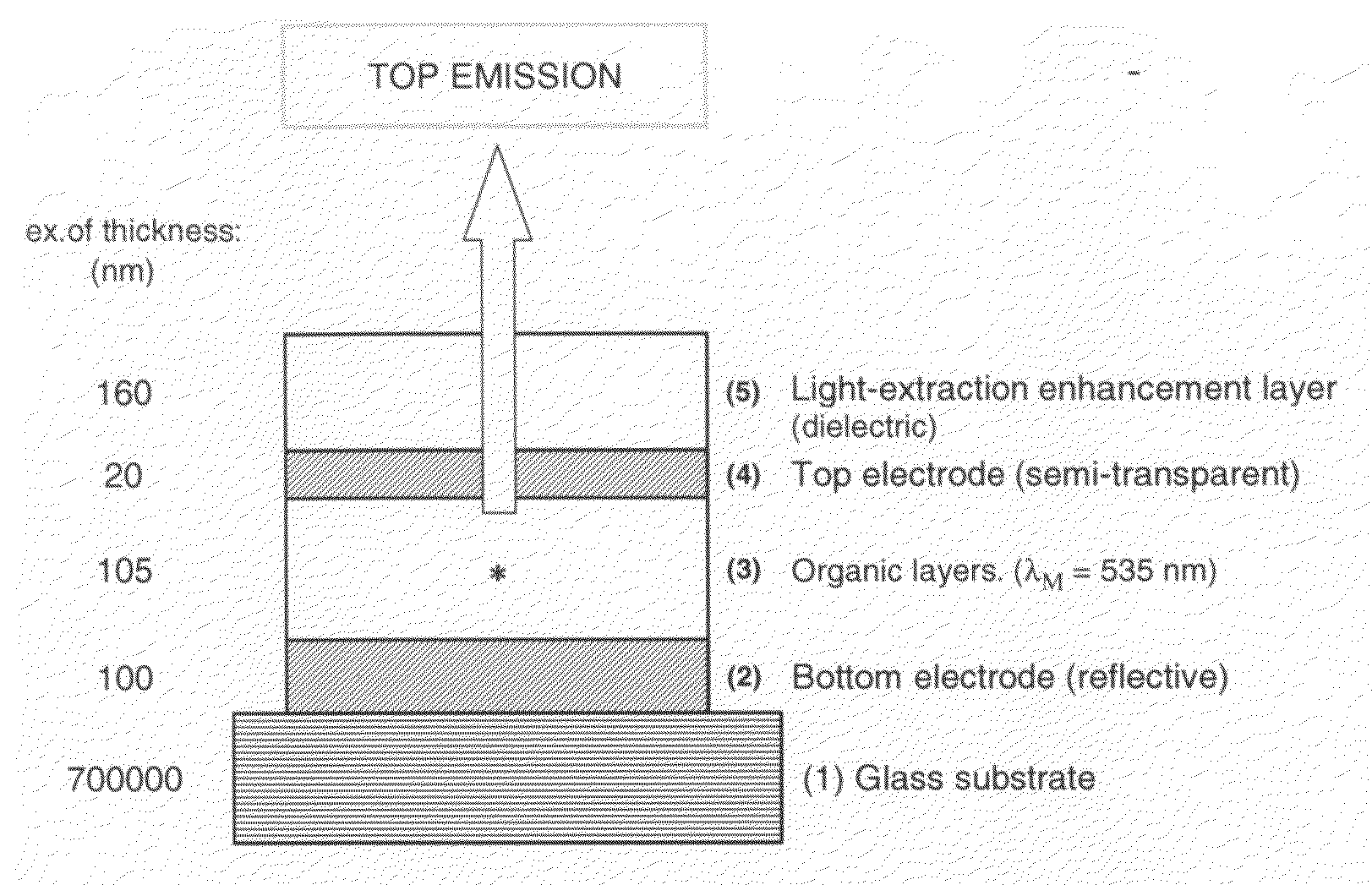
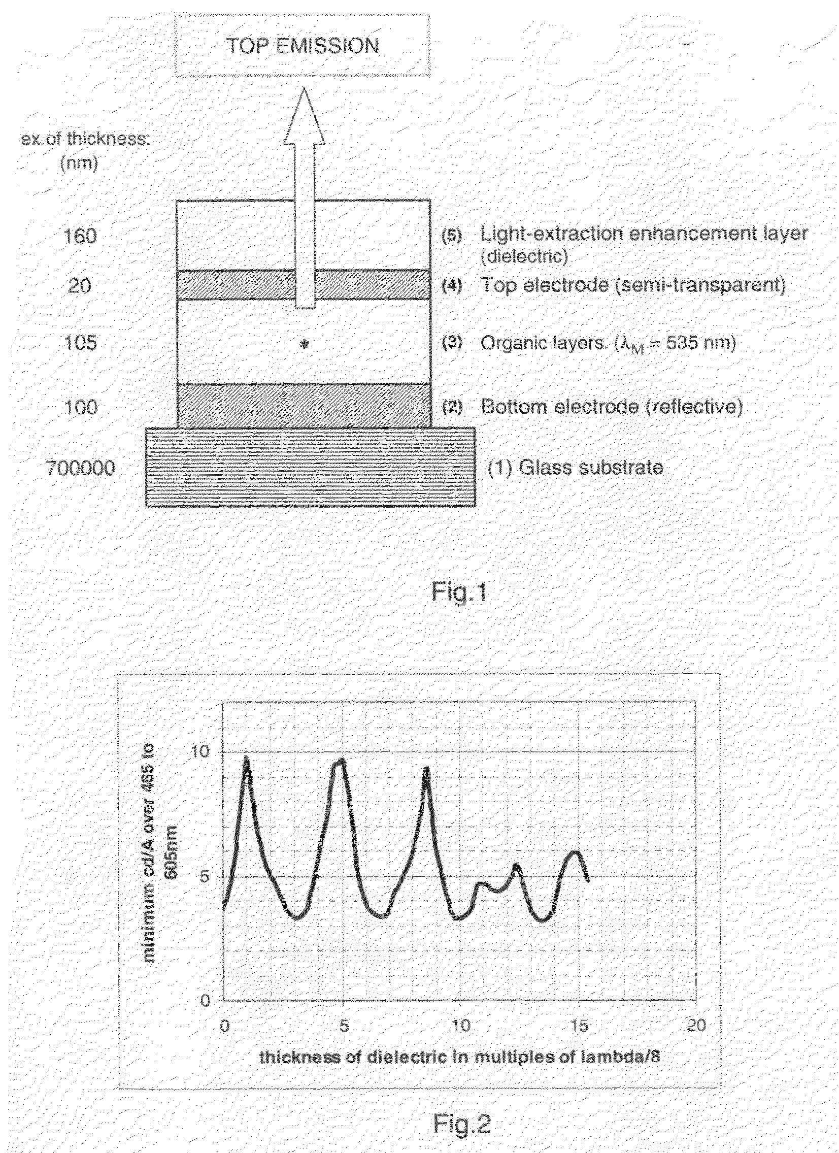
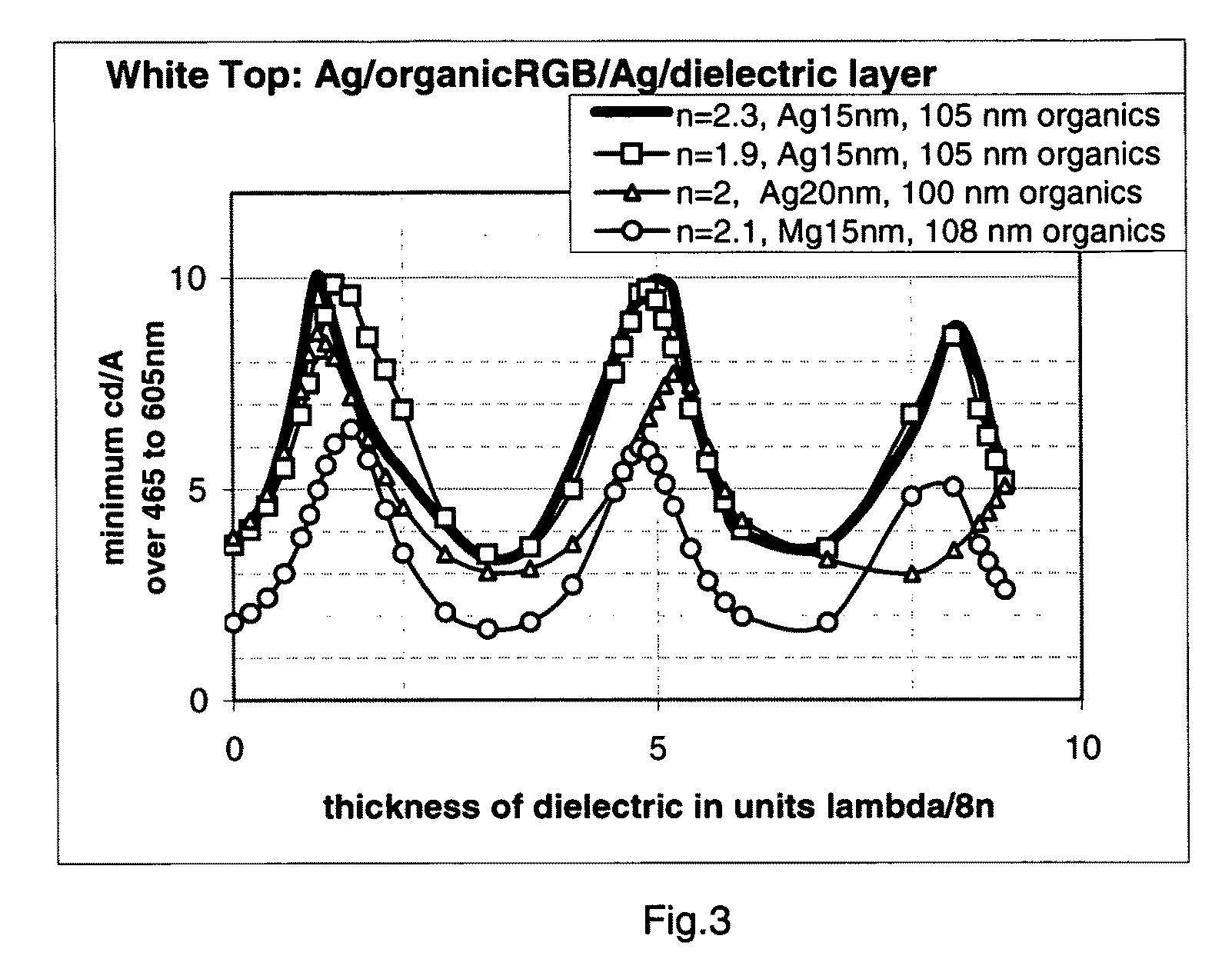
Oled or group of adjacent oleds with a light-extraction layer efficient over a large range of wavelengths
a light-extraction layer and light-extraction technology, applied in the field of organic light-emitting diodes (oled), can solve the problems of difficult application of light-extraction enhancement techniques, poor light-extraction enhancement techniques, and ineffective light-extraction enhancement techniques. achieve the effect of enhancing light extraction and improving light extraction
- Summary
- Abstract
- Description
- Claims
- Application Information
AI Technical Summary
Benefits of technology
Problems solved by technology
Method used
Image
Examples
reference example 1
White Bottom-Emitting Organic Diode According to Prior Art
[0033]A glass substrate 1 received from Asahi Glass (0.7 mm glass / 155 nm ITO polished / 230 nm Cr) is first cleaned in de-ionized water then patterned by photolithography (NMP strip); following these steps the active area is a free 3 mm disc of ITO, forming a bottom electrode 2 acting as an anode; on the inactive area, the ITO is covered by 290 nm of insulating resin (TELR-P003 from Tokyo Ohka Kogyo).
[0034]The resin is then hardened by baking at 200° C. during 30 minutes, the substrate is cleaned by de-ionized water, and dried at 200° C. during 5 minutes, then put under vacuum at 180° C. during 20 minutes, before entering the vacuum deposition equipment (Sunicel Plus equipment, base pressure of 70 μPa). The ITO is then subjected to plasma treatment under oxygen during 3 minutes.
[0035]A group of stacked organic layers 3 is then deposited. The first organic layer is a doped hole transport layer of 35 nm (a spiro compound doped wi...
example 1
White Bottom Emitting Organic Diode According to the Invention
[0039]The same Asahi substrate 1 as for the reference example 1 above is subjected to the same photolithography steps, except that the TELR resin is not deposited. After cleaning in de-ionized water and drying at 200° C. during 5 minutes+vacuum 180° C. during 20 minutes, the substrate) is transferred to the vacuum deposition equipment for deposition of a silver anode on top of the ITO layer. Here, the ITO layer is not necessary but used as a convenient base for its good surface smoothness. The ITO is subjected to plasma treatment under oxygen during 3 minutes, then an opaque layer of silver is deposited at 0.15 nm / s up to a thickness of 120 nm.
[0040]The silver layer is then subjected to 2.5 minutes of Ar plasma treatment, removed from the vacuum deposition equipment, and returns to the photolithography area for deposition of the same resin TELR; the active area of the bottom electrode 2 acting as an anode is now a free 3 ...
PUM
 Abstract
Description
Claims
Application Information


