

Large Scale Chemical Bath System and Method for Cadmium Sulfide Processing of Thin Film Photovoltaic Materials
a photovoltaic material and chemical bath technology, applied in the direction of thermoelectric device details, thermoelectric device final product manufacturing, etc., can solve the problems of petrochemical fuel supply limitation, rapid becoming a scarce resource, depletion, etc., and achieve the effect of cost-effective and easy-to-implement
- Summary
- Abstract
- Description
- Claims
- Application Information
AI Technical Summary
Benefits of technology
Problems solved by technology
Method used
Image

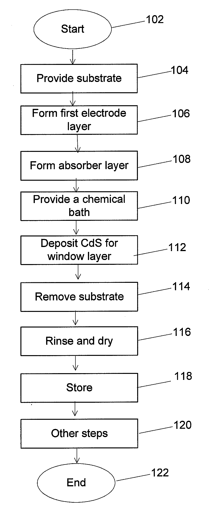
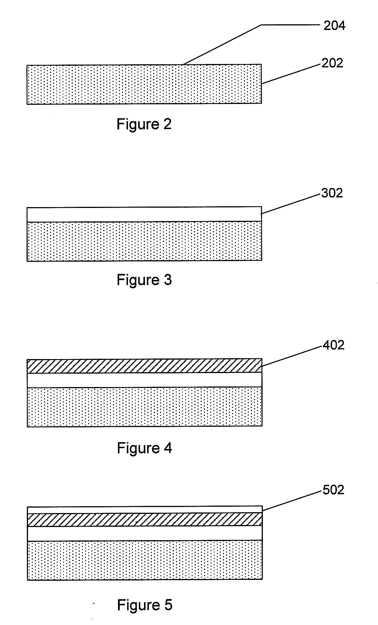
Examples
example 1
[0030]A solution comprising:
22.08 gm—Cadmium Acetate [Cd(CH3COO)2.2H2O]
6.58 gm—Thiourea
8.24 gm—Ammonium Chloride [NH4Cl]
6.0 l—Water
will form a uniform, continuous cadmium sulfide film. However, a solution having the same constituents in the same proportions, but without ammonium chloride, will not form such a film.
example 1-a
[0031]16.30 gm—Cadmium Acetate [Cd(CH3COO)2.2H2O]
6.58 gm—Thiourea
8.24 gm—Ammonium chloride [NH4Cl]
6.58 gm—Aluminum chloride [AlCl3.6H2O]
6.0 l—Water
[0032]This solution is essentially the same as the Example 1 solution, with the addition of aluminum chloride. The aluminum chloride is added to alter the physical properties of the cadmium sulfide film, in the manner and for the reasons disclosed in U.S. application Ser. No. 631,815. (U.S. Pat. No. 4,086,101)
example 1-b
[0033]29.45 gm—Cadmium Acetate [Cd(CH3COO)2.2H2O]
6.94 gm—Thiourea
14.0 ml HCl (concentrated)
6.0 l—Water
[0034]This solution, which is also essentially identical to the Example 1 solution, utilizes hydrochloric acid as the catalyzing chlorine containing compound, instead of ammonium chloride.
PUM
| Property | Measurement | Unit |
|---|---|---|
| thickness | aaaaa | aaaaa |
| volume | aaaaa | aaaaa |
| internal volume | aaaaa | aaaaa |
Abstract
Description
Claims
Application Information