Method for manufacturing composite piezoelectric substrate

a piezoelectric substrate and composite technology, applied in the direction of piezoelectric/electrostrictive transducers, instruments, transducer types, etc., can solve the problems of difficult design of vibration modes, inability to accurately control the orientation direction of a crystal axis, and severe limitations of piezoelectric films formed by the deposition method. to achieve the effect of efficient use of piezoelectric materials and uniform thickness

Active Publication Date: 2010-04-15
MURATA MFG CO LTD
View PDF10 Cites 95 Cited by
  • Summary
  • Abstract
  • Description
  • Claims
  • Application Information

AI Technical Summary

Benefits of technology

[0015]To overcome the problems described above, preferred embodiments of the present invention provide a method for manufacturing a composite pie

Problems solved by technology

However, a piezoelectric film formed by the deposition method has severe limitations on the materials that can be used due to the deposition temperature and deposition conditions for forming an oriented film, and AlN is primarily used.
Also, the orientation direction of a crystal axis cannot be accurately controlled, and a C-axis oriented film is primarily used, thereby causing difficulty in designing a vibration mode by inclining a piezoelectric axis.
On the other hand, a piezoelectric film that is formed by polishing a piezoelectric single crystal substrate results in most of the piezoelectric single crystal becoming polishing waste, thereby causing a low efficiency of material utilization.
Further, the thickness of the piezoelectric film depends on variations in the polishing speed and waviness of the substrate before polishing, and thus, it is difficult to accurately control the thickness so as to pr

Method used


Image

  • Method for manufacturing composite piezoelectric substrate
  • Method for manufacturing composite piezoelectric substrate
  • Method for manufacturing composite piezoelectric substrate

Examples


Embodiment Construction

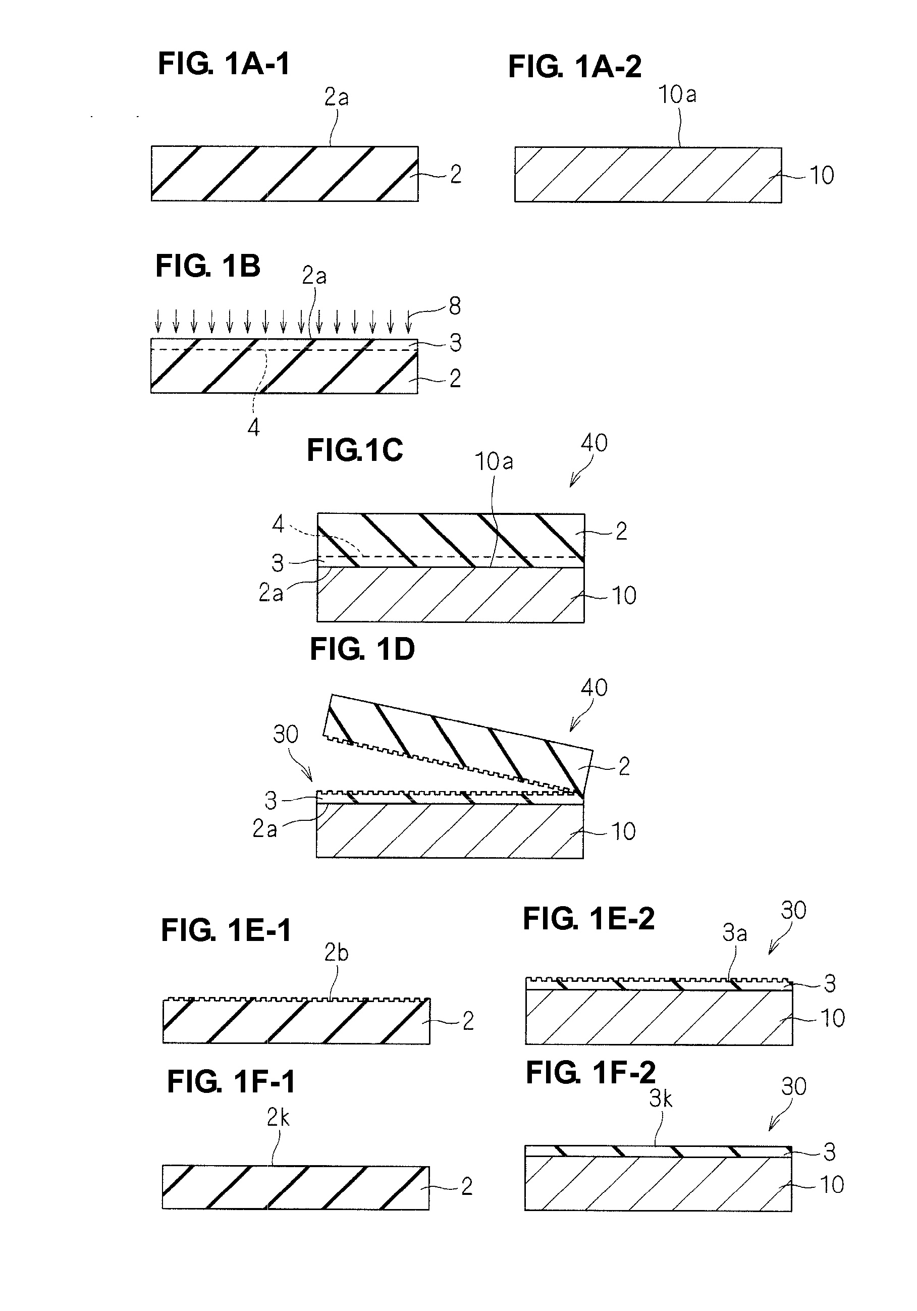
[0036]Preferred embodiments of the present invention are described with reference to FIGS. 1A-1 through FIG. 5B.

[0037]A method for manufacturing a surface acoustic wave (SAW) device a preferred embodiment of the present invention is described with reference to FIGS. 1A-1 through FIG. 5B.

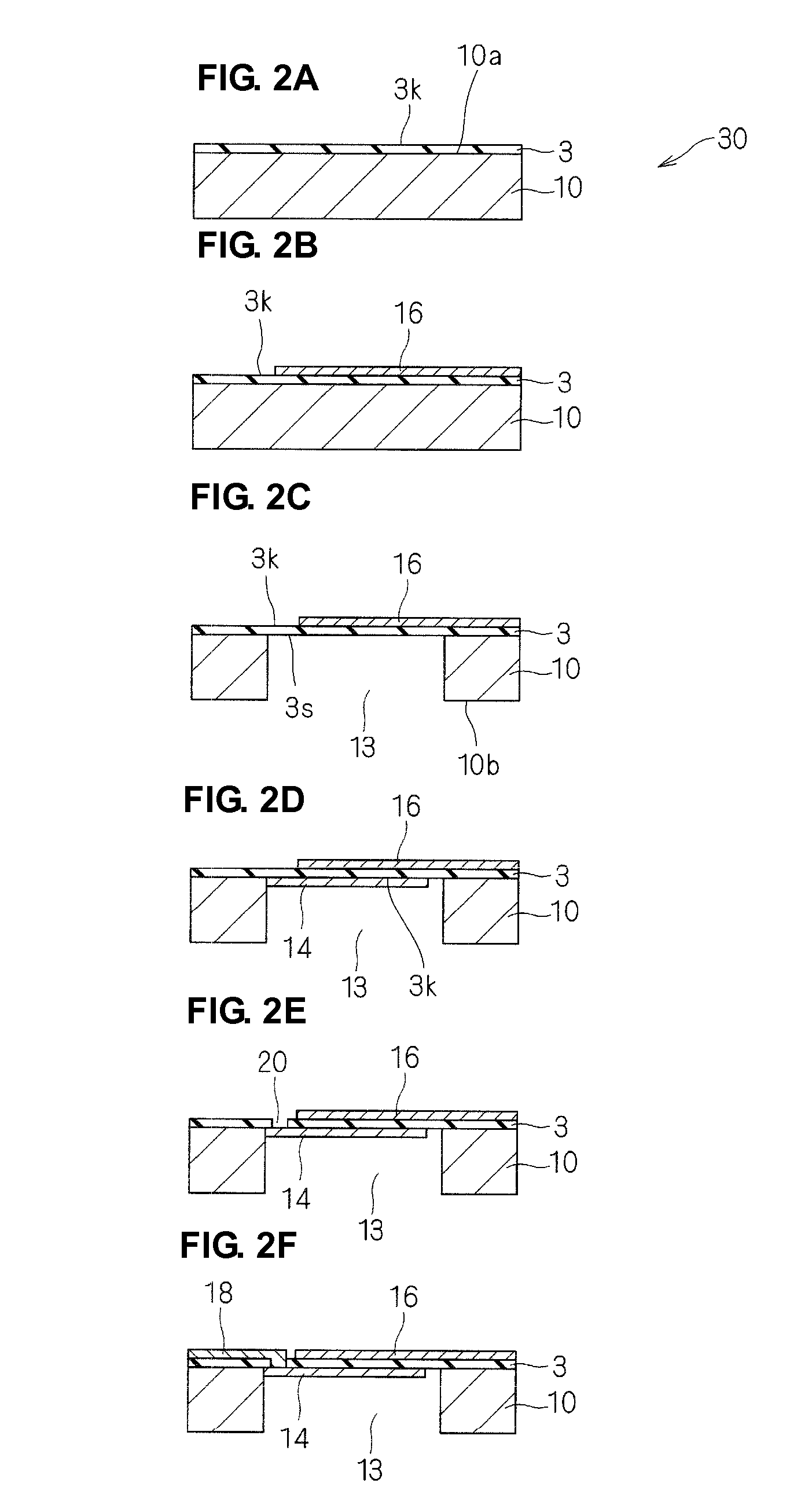
[0038]First, steps for manufacturing a composite piezoelectric substrate 30 used in a SAW device are described with reference to FIGS. 1A-1 through 1F-2, which are sectional views showing steps for manufacturing the composite piezoelectric substrate 30.

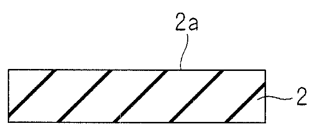
[0039]As shown in FIGS. 1A-1 and 1A-2, a piezoelectric substrate 2 and a supporting substrate 10 are prepared. For example, a 42° Y-cut LiTaO3 substrate is preferably prepared as the piezoelectric substrate 2, and a Si substrate is preferably prepared as the supporting substrate 10. Surfaces 2a and 10a of the substrates 2 and 10, respectively, are previously polished to mirror surfaces.

[0040]Next, as shown by arrows 8 in FIG. 1B, ions are implanted int...


PUM

PropertyMeasurementUnit
Thicknessaaaaaaaaaa
Piezoelectricityaaaaaaaaaa

Abstract

A method for manufacturing a composite piezoelectric substrate is capable of forming an ultra-thin piezoelectric film having a uniform thickness by efficiently using a piezoelectric material. A piezoelectric substrate and a supporting substrate are prepared, ions are implanted from a surface of the piezoelectric substrate to form a defective layer in a region at a predetermined depth from the surface of the piezoelectric substrate, impurities that are adhered to at least one of the surface of the piezoelectric substrate in which the defective layer is formed and a surface of the supporting substrate are removed to directly expose the constituent atoms of the surfaces and to activate the surfaces, the supporting substrate is bonded to the surface of the piezoelectric substrate to form a bonded substrate body, the bonded substrate body is separated at the defective layer formed in the piezoelectric substrate so that a separation layer between the surface of the piezoelectric substrate and the defective layer is separated from the piezoelectric substrate and bonded to the supporting substrate to form a composite piezoelectric substrate, and the surface of the separation layer of the composite piezoelectric substrate is smoothed.

Description

BACKGROUND OF THE INVENTION[0001]1. Field of the Invention[0002]The present invention relates to a method for manufacturing a composite piezoelectric substrate, and particularly, to a method for manufacturing a composite piezoelectric substrate including a piezoelectric film.[0003]2. Description of the Related Art[0004]Recently, filters using ultra-thin piezoelectric materials, such as ultra-thin piezoelectric films, have been actively developed. Although AlN thin films and ZnO thin films formed by a deposition method, such as a sputtering method, a CVD method, or other suitable method are generally used as the ultra-thin piezoelectric films in filters and other similar devices, any one of the films can be a C-axis oriented film in which the C-axis is aligned in the vertical direction of a substrate.[0005]On the other hand, it has been proposed to manufacture a composite piezoelectric substrate including a piezoelectric film by bonding a piezoelectric single crystal substrate to a s...

Claims


Application Information

Patent Timeline
IPC IPC(8): H01L41/22H01L41/257H01L41/312
CPCH03H3/02H03H2003/021H03H2003/023Y10T29/42H01L41/312H01L41/27H01L41/257H01L21/76254Y10T29/49005Y10T29/49155G02F1/035H10N30/045H10N30/072H03H3/08H03H9/25H03H2003/027H10N30/05H10N30/085H10N30/086H10N30/853H10N30/03
Inventor KANDO, HAJIMEYOSHII, YOSHIHARU
Owner MURATA MFG CO LTD
Why Eureka
Try Eureka