

Film depositing apparatus, a film depositing method, a piezoelectric film, and a liquid ejecting apparatus
- Summary
- Abstract
- Description
- Claims
- Application Information
AI Technical Summary
Benefits of technology
Problems solved by technology
Method used
Image

Examples
embodiment 1
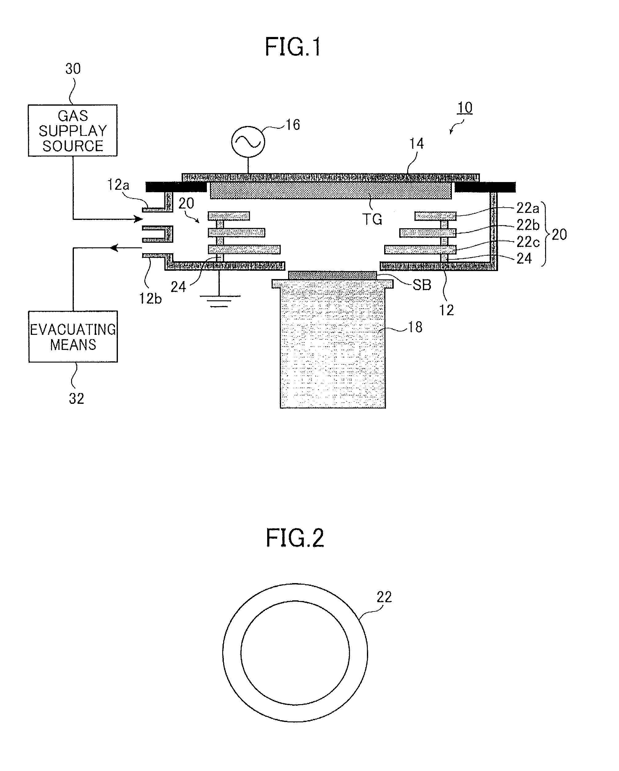
[0025]FIG. 1 shows the structure of a film depositing apparatus generally indicated at 10 according to Embodiment 1 of the present invention.
[0026]On the following pages, a film depositing apparatus that deposits a piezoelectric film as a thin layer and which produces a piezoelectric device as a thin-film device that uses the thin layer is described as a typical example but it should be noted that the present invention is by no means limited to this particular case and that it is also applicable in film depositing apparatuses that produce other types of thin-film devices.
[0027]As shown in FIG. 1, the film depositing apparatus 10 has a vacuum vessel (process chamber) 12 which has a target holder 14 placed on its ceiling portion. The target holder 14 not only holds a sputter target material TG but also functions as a cathode for generating a plasma within the vacuum vessel 12. The target holder 14 is connected to a RF power supply 16. Beneath the area of the vacuum vessel 12 in a face...
embodiment 2
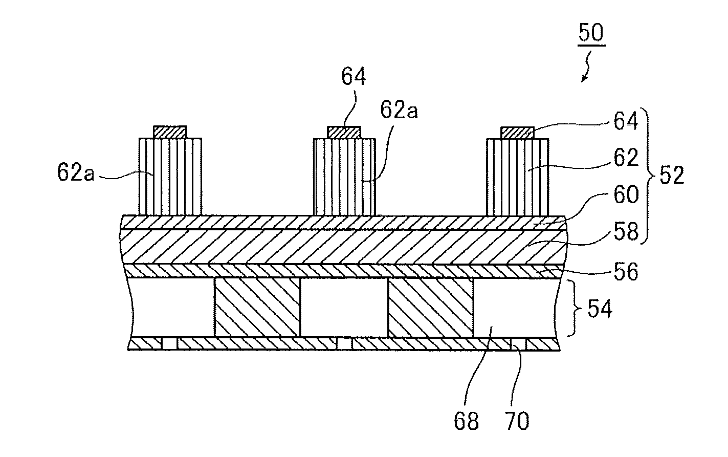
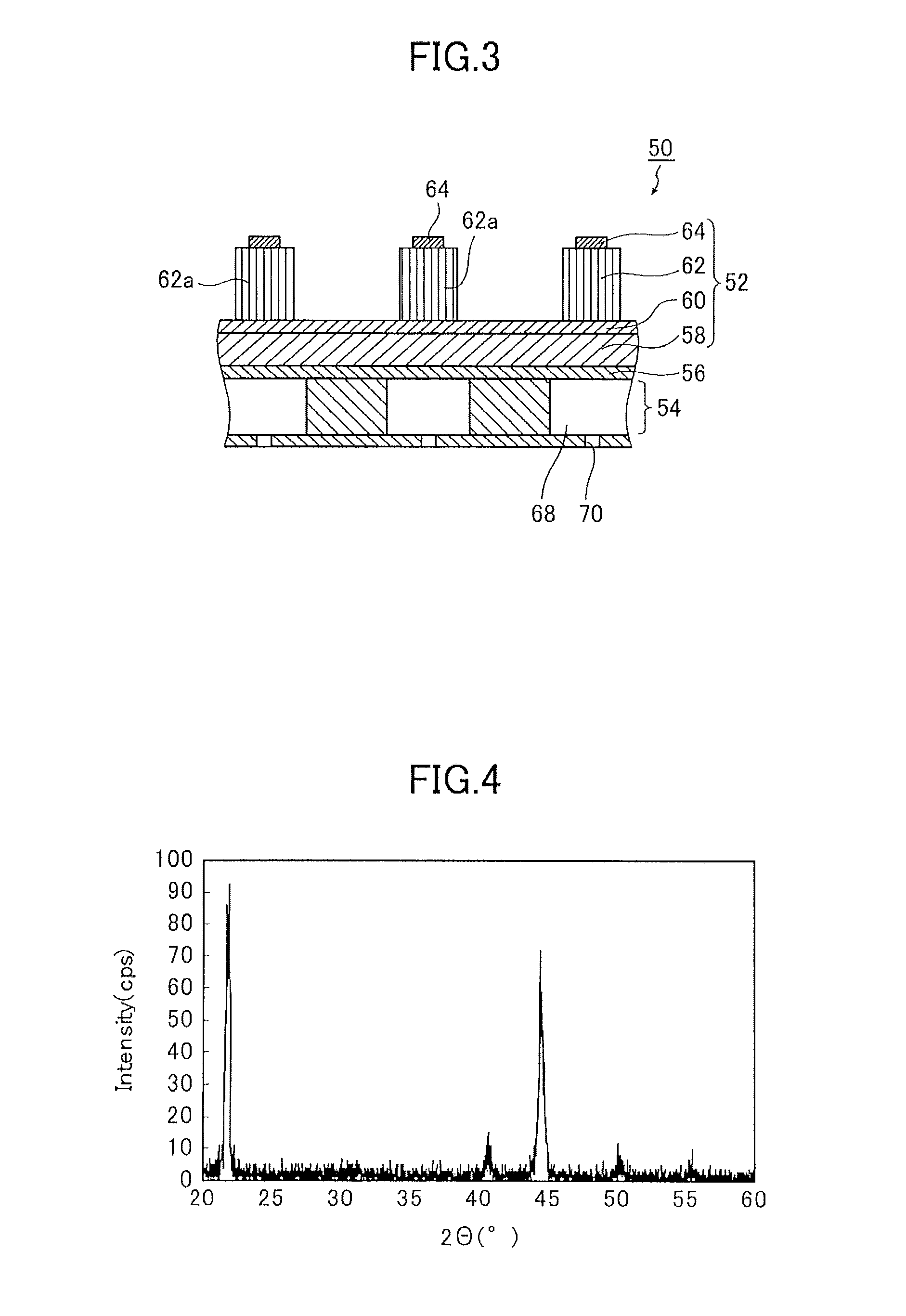
[0074]FIG. 3 is a sectional view showing the essential parts of an ink-jet head (liquid ejecting apparatus) generally indicated by 50 according to Embodiment 2 of the present invention, with the section being taken across the thickness of the piezoelectric device. For clarity purposes, the individual components are not scaled to the actual model but are altered as appropriate.
[0075]The ink-jet head 50 comprises a piezoelectric device 52 having the piezoelectric film of the present invention, an ink storing / ejecting member 54, a diaphragm 56 provided between the piezoelectric device 52 and the ink storing / ejecting member 54, and nozzles (liquid ejecting ports) 70.
[0076]The piezoelectric device 52 comprises a substrate 58 on which a lower electrode 60, a piezoelectric film 62 and upper electrodes 64 are superposed in that order; they are so designed that the lower electrode 60 and each of the upper electrode 64 together apply an electric field to the piezoelectric film 62 across its t...
example 1
[0088]As the film depositing apparatus 10 shown in FIG. 1, used was an apparatus of a commercial type (Model CLN 2000 of Oerlikon).
[0089]The target material TG was a sintered disk of 300 mm diameter with the composition of Pb1.3(Zr0.52Ti0.48)O3.
[0090]The substrate SB had a size of 6 inch diameter and consisted of a Si wafer with an Ir coat formed preliminarily in a thickness of 150 nm.
[0091]The distance between the target material TG and the substrate SB was set at 50 mm.
[0092]Anode 20 was placed over the substrate SB in such a way that it surrounded the outer periphery of the side of the substrate SB facing the target material TG; the anode consisted of three stainless steel (SUS) plate members 22a, 22b and 22c; the plate member 22a was the closest to the target material TG and had an outside diameter of 300 mm and an inside diameter of 260 mm; the plate member 22b was beneath the plate member 22a as seen in FIG. 1 and had an outside diameter of 300 mm and an inside diameter of 220...
PUM
| Property | Measurement | Unit |
|---|---|---|
| Distance | aaaaa | aaaaa |
| Distance | aaaaa | aaaaa |
| Piezoelectric constant | aaaaa | aaaaa |
Abstract
Description
Claims
Application Information