Phase correction circuit of encoder signal
a phase correction circuit and encoder technology, applied in the field of phase correction circuit of encoder signal, can solve the problems of deteriorating position detection accuracy, affecting the accuracy of phase correction, and limiting the resolution of the method in terms of processing accuracy or optical diffraction effect,
- Summary
- Abstract
- Description
- Claims
- Application Information
AI Technical Summary
Benefits of technology
Problems solved by technology
Method used
Image
Examples
first embodiment
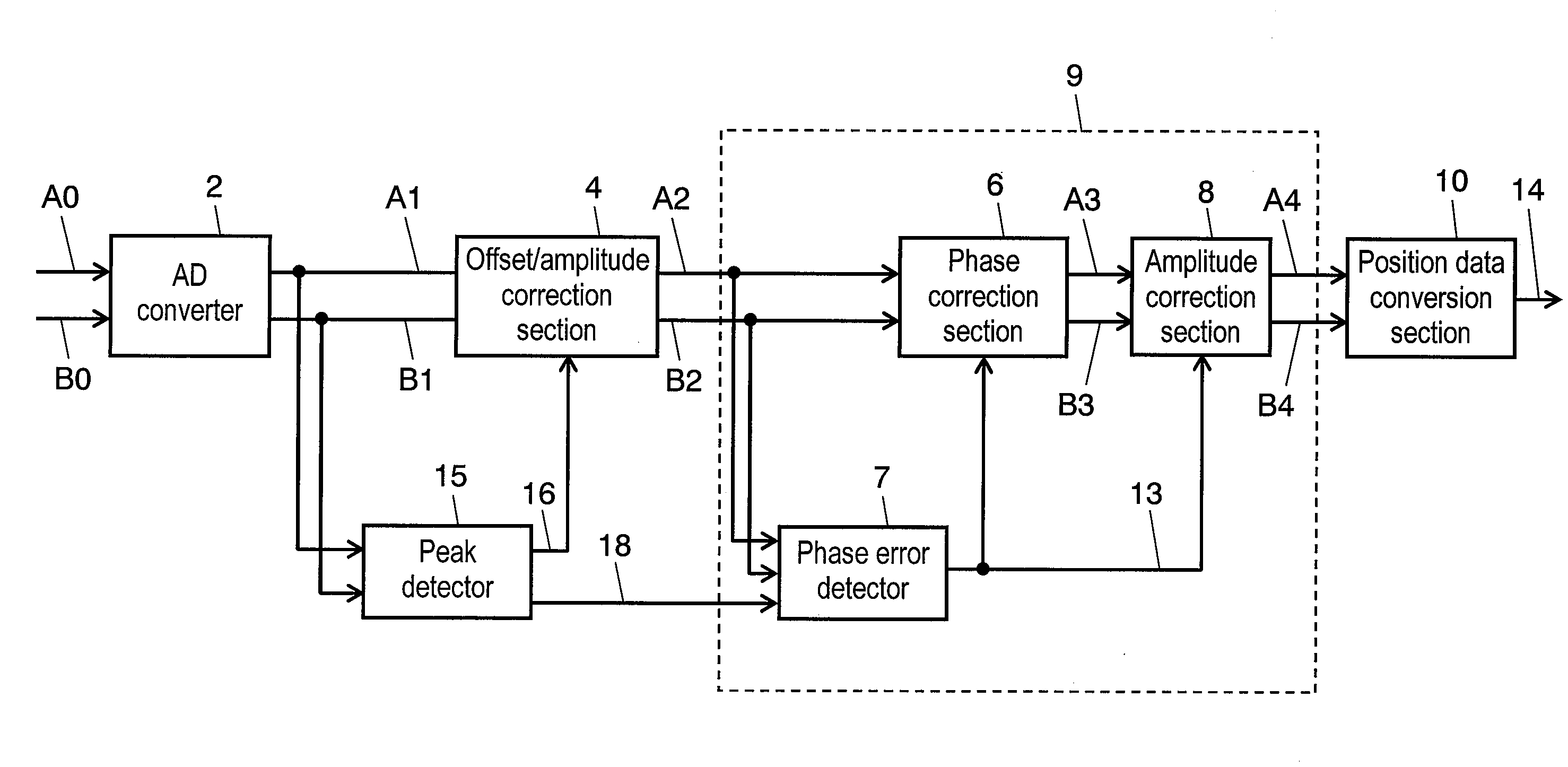
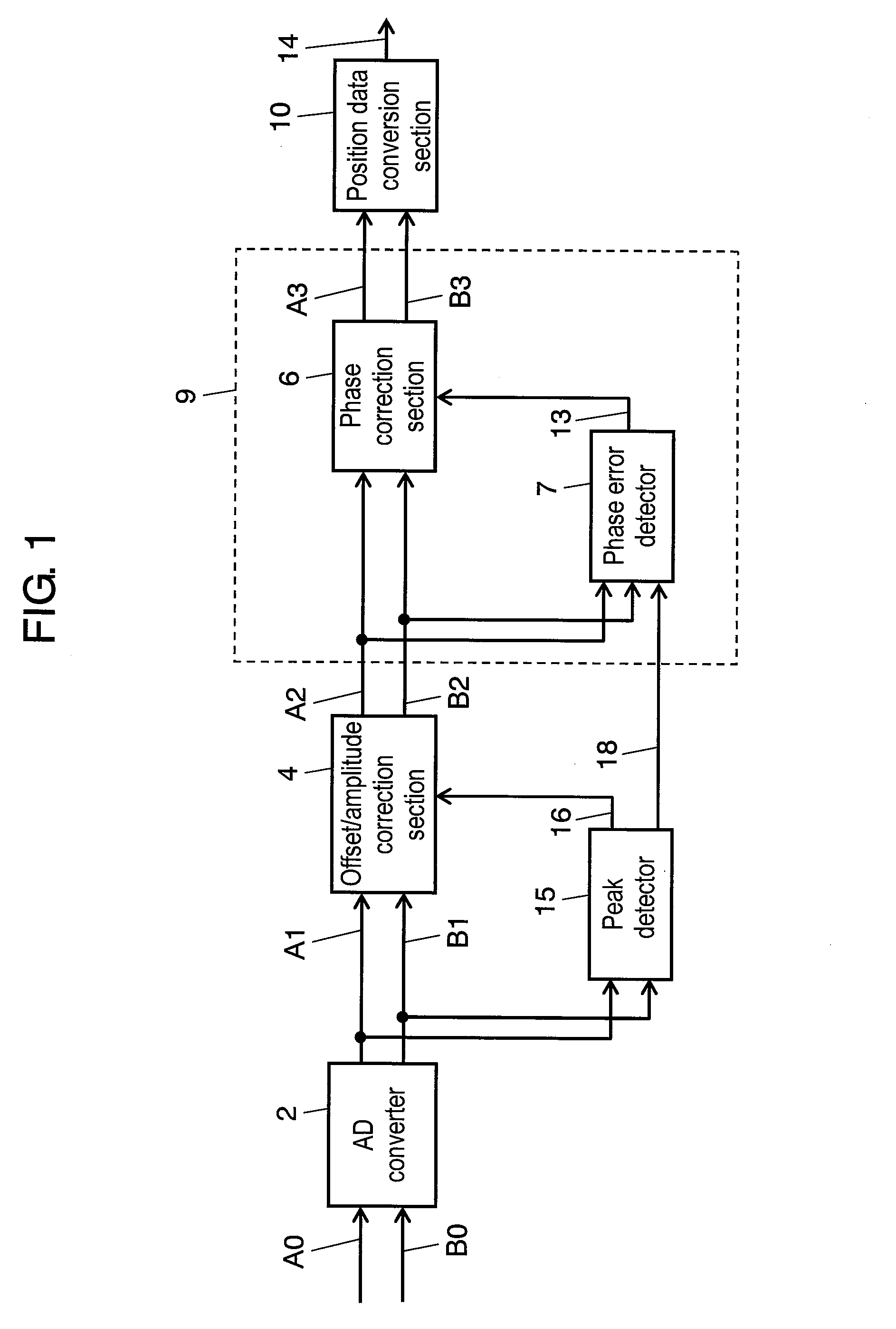
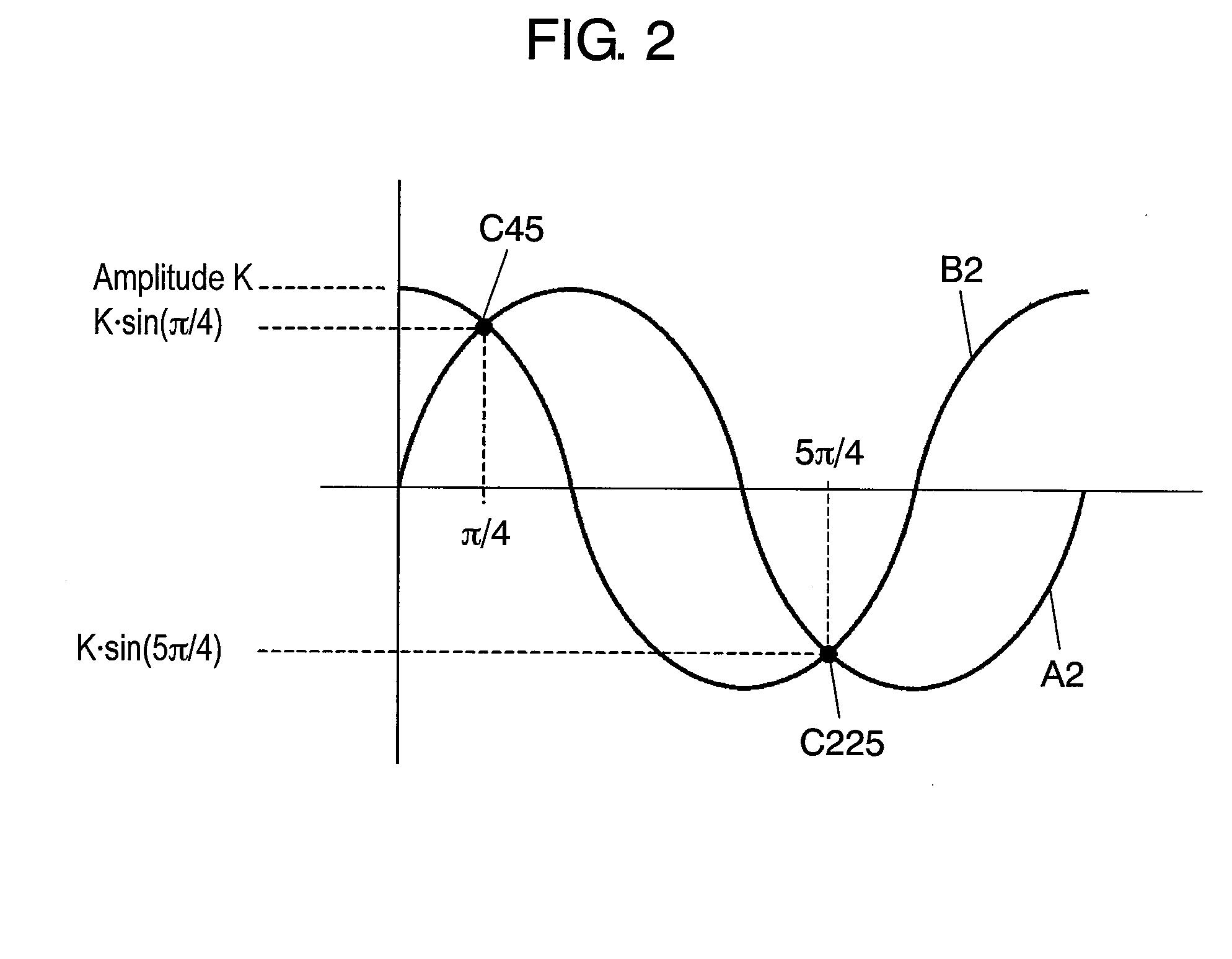
[0046]A phase correction circuit of an encoder signal in accordance with the present invention is described with reference to FIGS. 1 to 6. FIG. 1 is a block diagram illustrating an encoder signal processing circuit and FIGS. 2 to 6 illustrate operation waveforms of phase error detection.
[0047]In FIG. 1, an analog A0 signal and an analog B0 signal in the original signals output from an encoder are sinusoidal signals of an A phase and a B phase having a phase difference of 90 degrees. In general, the encoder is constructed with a light emitting device, a light receiving device, and a slit plate.
[0048]The light emitting device uses a light emitting diode (LED) or laser beam and the light receiving device uses a photo diode or photo transistor. The slit plate is made of a resin material or a glass for transmitting light. A grid pattern mask for blocking light is provided on the slit plate. Arrangement is made such that the light receiving device receives the transmitted light from the ...
second embodiment
[0077]The second embodiment of the present invention is described with reference to FIGS. 7 and 8. The second embodiment is different from the first embodiment in that an inverted signal of one side of two phase signals is used for error detection of phase error detector 7 and this difference is described below.
[0078]Like FIG. 2, FIG. 7 illustrates waveforms of the A2 signal and the B2 signal for which an offset correction process and an amplitude correction process have been performed. FIG. 7 is different from FIG. 2 in that an inverted signal of the B2 signal is generated and intersection points C135 and C315 are present between the inverted signal and the A2 signal.
[0079]FIG. 8 illustrates the B2d signal in which the phase of the B2 signal between the A2 and B2 signals is advanced by α radian. Since intersection points C45 and C225 can be detected in the structure equal to that of the first embodiment, a method for detecting intersection points C135 and C315 is described.
[0080]Th...
third embodiment
[0083]The third embodiment of the present invention is described with reference to FIG. 9. The third embodiment is different from the first and second embodiments in that peak values of two phase signals are used at error detection points of phase error detector 7 and this difference is described below.
[0084]Like FIG. 3, FIG. 9 illustrates waveforms of the A2 signal and the B2d signal for which an offset correction process and an amplitude correction process have been performed. The B2d signal is the case where the ideal B2 signal is shifted by a phase of α radian.
[0085]Phase error detection points are those at which peak values of the A2 signal and the B2d signal are detected. These points can be detected by peak detector 15 from the A1 signal and the B1 signal whose peak points are identical. If the A2 signal and the B2d signal are two ideal phase signals having a phase difference of 90 degrees, one signal is 0 at the peak points of the signals. However, when a phase error is pres...
PUM
 Abstract
Description
Claims
Application Information


