Printed wiring board and method for manufacturing the same

a printing method and wiring board technology, applied in the direction of resist details, printed circuit aspects, printed circuit manufacturing, etc., can solve the problems of reducing yield, difficult to reduce the diameter b>1/b> of the connecting pad, and inability to make the diameter equal, etc., to facilitate the manufacturing of printed wiring boards

Inactive Publication Date: 2010-04-22
IBM CORP
View PDF6 Cites 14 Cited by
  • Summary
  • Abstract
  • Description
  • Claims
  • Application Information

AI Technical Summary

Benefits of technology

[0018]The present invention facilitates manufacturing a printed wiring board having brimmed-hat-shaped connecting pads.

Problems solved by technology

However, those diameters cannot be made equal because of the following reasons.
This makes it difficult, in forming the under bump metals 11 by plate patterning, to remove unnecessary plate in the area other than the under bump metals 11, which reduces yields.
On the other hand, it is also difficult to reduce the diameter φ1 of the connecting pad 5.
However, since the protruding conductors protrude from the wiring board, it is difficult to make the diameter of the joint sur

Method used


Image

  • Printed wiring board and method for manufacturing the same
  • Printed wiring board and method for manufacturing the same
  • Printed wiring board and method for manufacturing the same

Examples


Embodiment Construction

[0058]Embodiments of the present invention will be described in detail below with reference to the drawings. In the drawings, like or corresponding parts are given like reference numerals and descriptions thereof will not be repeated.

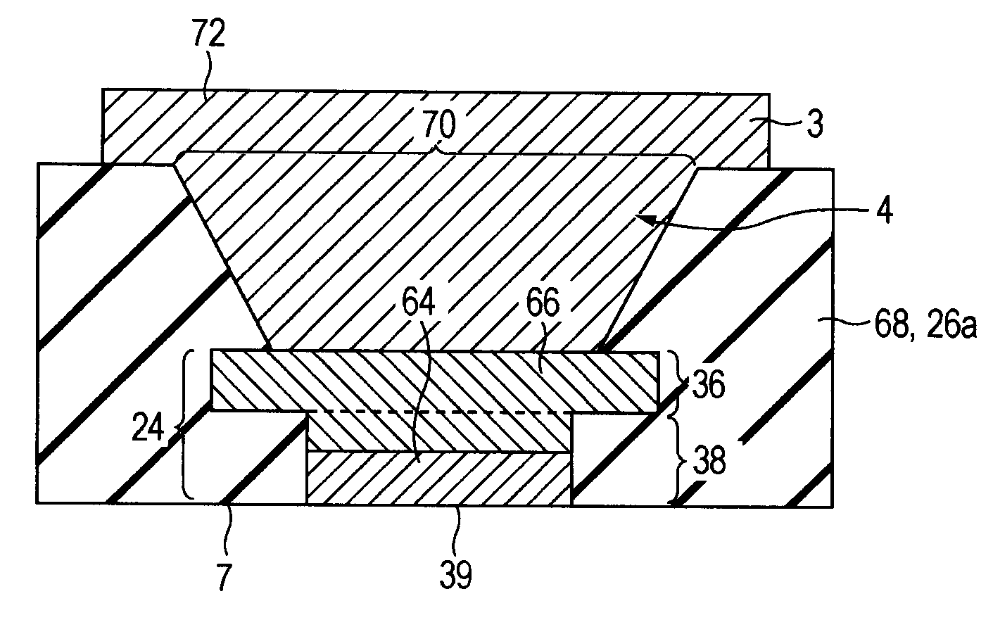
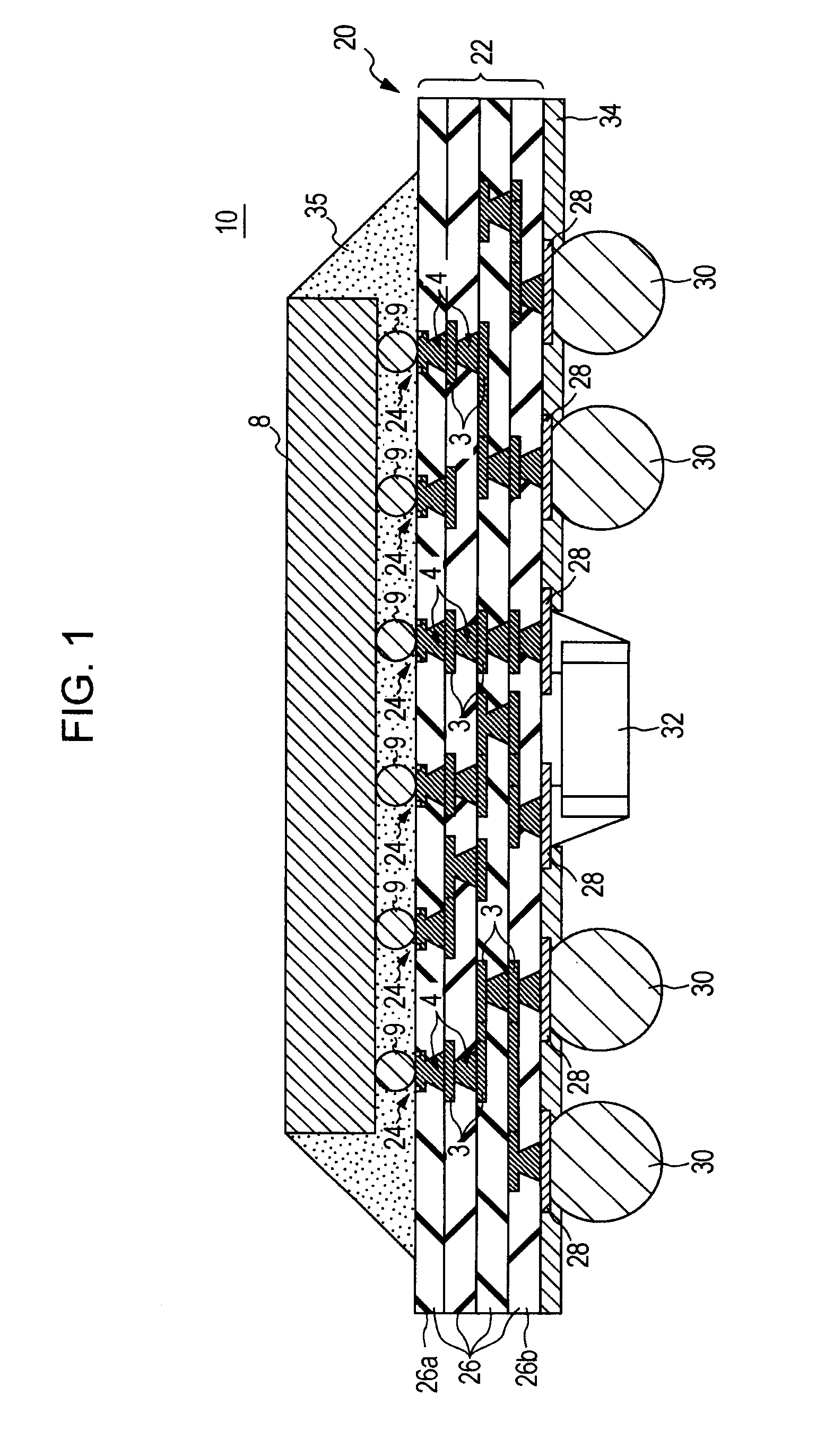
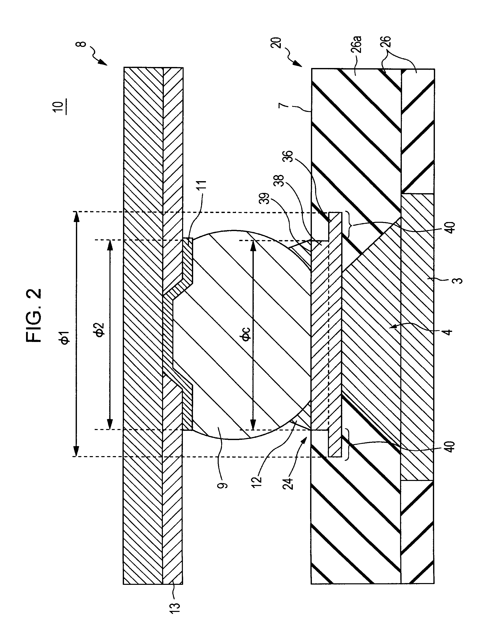
[0059]Referring to FIG. 1, a semiconductor package 10 according to an embodiment of the present invention includes a coreless substrate 20 and a semiconductor chip 8 mounted on the coreless substrate 20. The coreless substrate 20 includes a build-up layer 22, a plurality of lands 3, a plurality of vias 4, and a plurality of connecting pads 24. The build-up layer 22 is formed a plurality of stacked dielectric layers 26. The lands 3 are shaped like a column (a thin disc) and are completely embedded in the dielectric layers 26, where they are connected to wiring layers in the dielectric layers 26. The vias 4 are shaped like a column or a truncated cone and are completely embedded in the dielectric layers 26. The vias 4 are each formed between the land 3 an...


PUM

PropertyMeasurementUnit
Dielectric polarization enthalpyaaaaaaaaaa

Abstract

Embodiments of the present invention provide a printed wiring board in which solder bumps of a mounted semiconductor chip are less prone to be ruptured. The printed wiring board includes a coreless substrate which includes: a dielectric layer having a main surface and a connecting pad embedded in the dielectric layer. The connecting pad is shaped like a brimmed hat. That is, the connecting pad includes a plate portion whose diameter φ1 is about 95 μm and a contact portion whose diameter φc is about 75 μm. The main surface of the contact portion is exposed at the main surface of the dielectric layer. Since diameter φc of the contact portion is substantially the same as diameter φ2 of an under bump metal at the semiconductor chip side, even if mechanical stress is applied in a direction in which the semiconductor chip is peeled off from the coreless substrate, the stress disperses evenly to both of the connecting pad and the under bump metal, and thus rupture is less prone to occur.

Description

CROSS-REFERENCE TO RELATED APPLICATION[0001]The present application claims the benefit of priority of a Japanese Patent Application No. 2008-271265, filed Oct. 21, 2008 with the Japan Patent Office, the content of which is incorporated herein by reference in its entirety.FIELD OF THE INVENTION[0002]The present invention relates to a printed wiring board and a method for manufacturing the same, and more specifically, to a coreless substrate having no core substrate, a semiconductor package, and a method for manufacturing the same.BACKGROUND OF THE INVENTION[0003]U.S. Pat. No. 5,926,798 (Patent Document 1) discloses a flip-chip mount technology using a controlled collapse chip connection (C4) technology. This technology is a method for mounting a semiconductor chip (IC chip) on a printed wiring board. A semiconductor chip to be mounted has an array of a large number of solder bumps.[0004]FIG. 14 is an enlarged cross-sectional view of the vicinity of a solder bump of a semiconductor pa...

Claims


Application Information

Patent Timeline
IPC IPC(8): H01L23/48H05K1/11H01K3/10H01L21/60
CPCH01L21/4853Y10T29/49124H01L23/49816H01L23/49822H01L23/50H01L24/16H01L2224/16225H01L2924/01078H01L2924/01079H01L2924/14H01L2924/15311H01L2924/19041H01L2924/19106H01L2924/3025H05K1/113H05K3/205H05K3/4007H05K3/421H05K3/4682H05K2201/09845H05K2201/09854H05K2203/0574H01L2224/16227H01L2224/32225H01L2224/73204H01L23/49811Y10T29/49162H01L2924/00H01L2224/05573H01L2224/05572H01L2924/00012H01L2224/05647H01L2924/00014H01L2224/05666H01L2224/05671H05K3/46
Inventor MORI, HIROYUKIKAWASAKI, KAZUSHIGE
Owner IBM CORP
Why Eureka
Try Eureka