
Package module structure of compound semiconductor devices and fabricating method thereof

a technology of compound semiconductor devices and package modules, which is applied in the direction of semiconductor devices, semiconductor device details, semiconductor/solid-state device details, etc., can solve the problems of poor heat dissipation, inconvenient heat dissipation path, and inability to heat-transfer to high-power chemical compound semiconductor devices, etc., to achieve effective dissipation of heat, reduce manufacturing costs, and reduce manufacturing costs

Inactive Publication Date: 2010-04-22
ADVANCED OPTOELECTRONICS TECH
View PDF12 Cites 20 Cited by
  • Summary
  • Abstract
  • Description
  • Claims
  • Application Information

AI Technical Summary

Benefits of technology

[0008]One aspect of the present invention provides a package module structure of compound semiconductor devices and a fabricating method thereof. The package module structure of compound semiconductor devices has a heat dissipation film for effectively dissipating heat, so as to resolve the poor heat dissipation problem. Moreover, by using a thin substrate, the package module structure of compound semiconductor devices can be made thinner for saving space.

Problems solved by technology

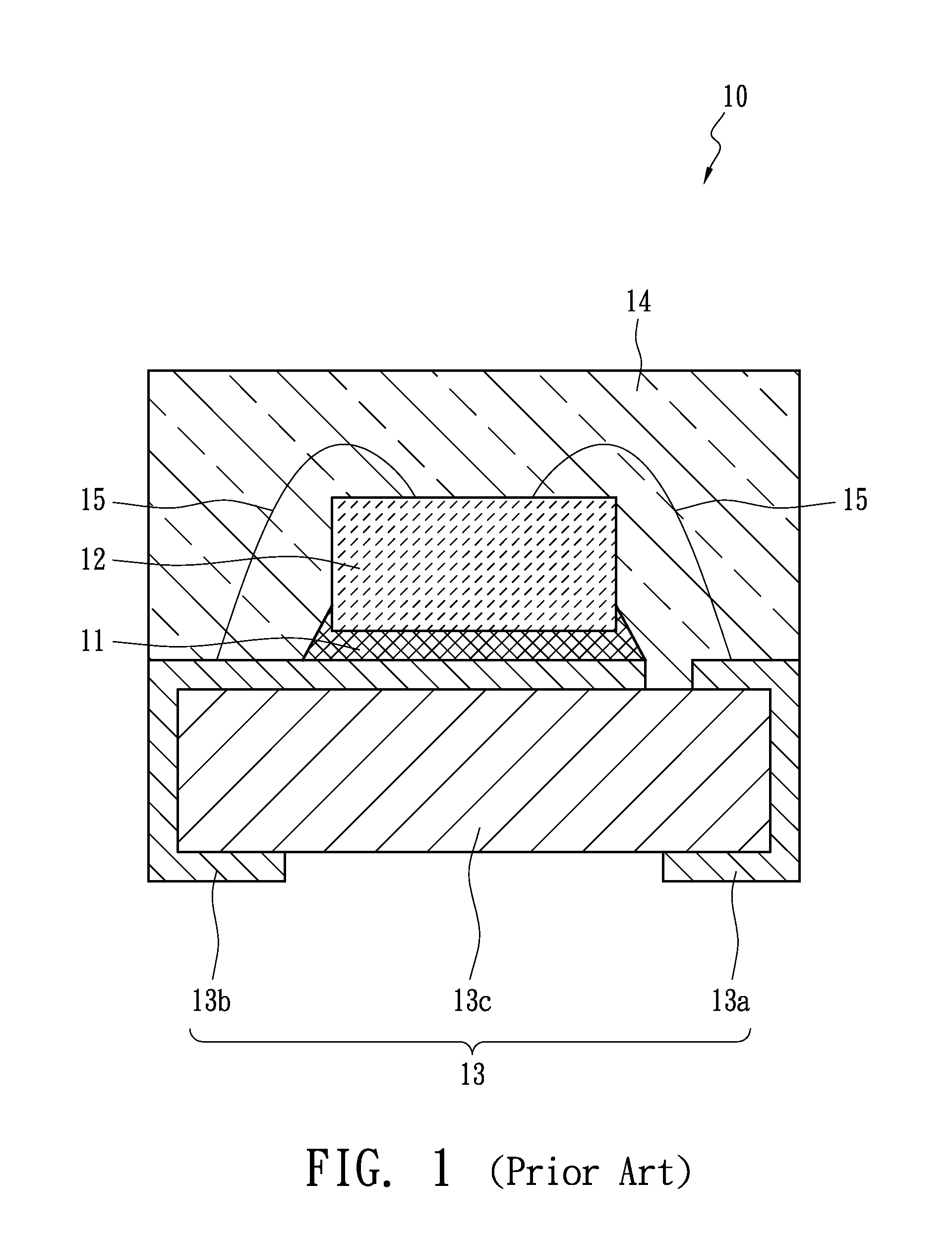
In addition, the insulation layer 13c is made mostly of epoxy resin with poor heat dissipation, and therefore is not suitable for a high power chemical compound semiconductor device as a heat-transferring path.
If plural LED devices 10 constitute an LED module, a more serious heat dissipation problem may occur.

Method used


Image

  • Package module structure of compound semiconductor devices and fabricating method thereof
  • Package module structure of compound semiconductor devices and fabricating method thereof
  • Package module structure of compound semiconductor devices and fabricating method thereof

Examples


first embodiment

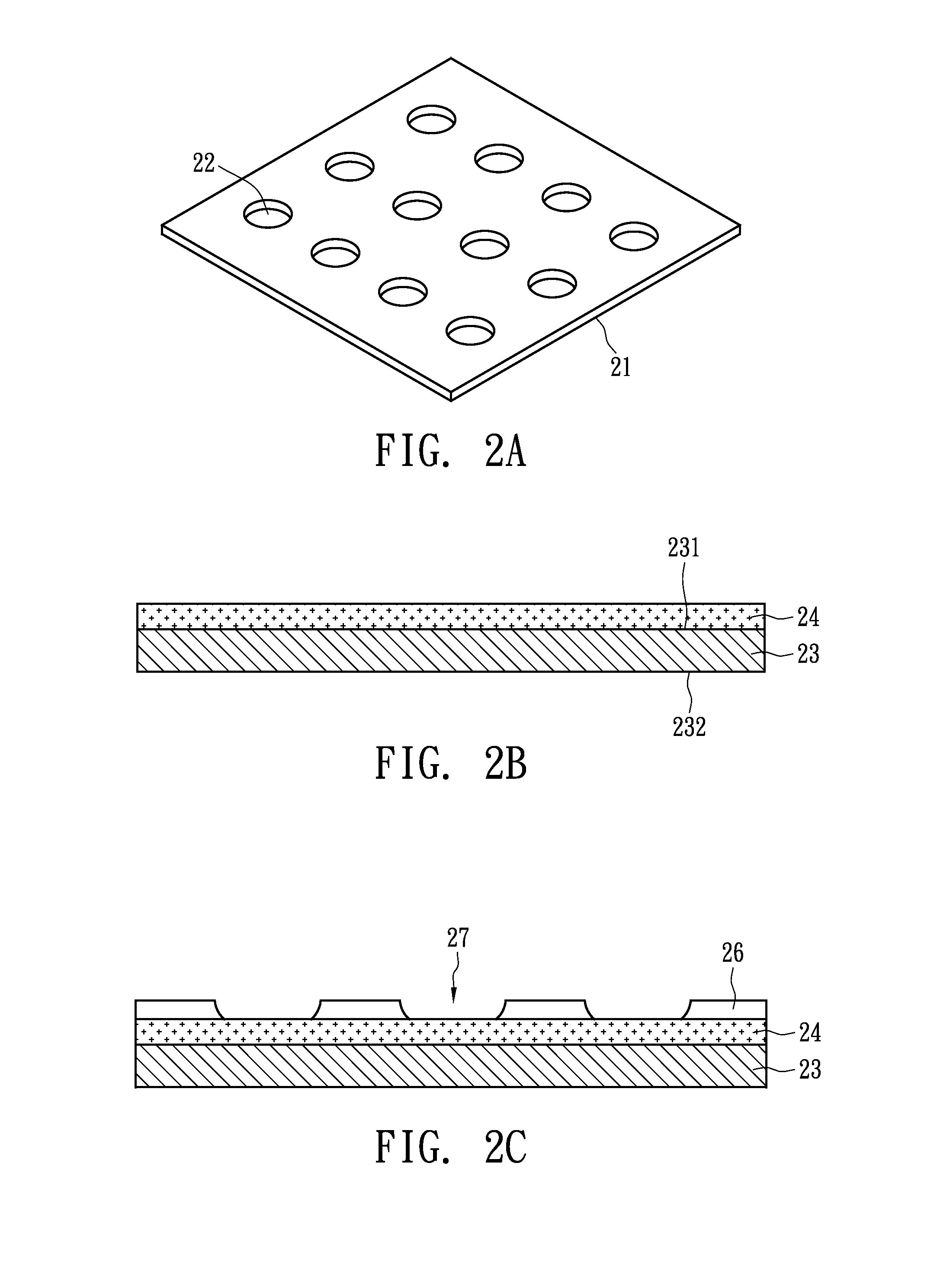
[0019]FIGS. 2A through 2H are schematic illustrations showing the manufacturing steps of the package module structure of compound semiconductor devices in accordance with the present invention. FIG. 2A shows a circuit board 21 with holes 22. In an embodiment, the circuit board 21 is a flexible printed circuit (FPC), e.g., FR-4, and is prepared in advance as a component for sequentially fabricating the package module structure of compound semiconductor devices.

[0020]In FIG. 2B, a temporary substrate 23 includes a first surface 231 and a second surface 232. In this drawing, the first surface 231 is an upper surface and the second surface 232 is a lower surface. The temporary substrate 23 may be made of a metallic material, a ceramic material or a polymer material. A heat dissipation film 24 is formed on the first surface 231 of the temporary substrate 23. The heat dissipation film 24 may be a metallic film without a circuit pattern and may be made of silver, nickel, copper, tin, alumi...

second embodiment

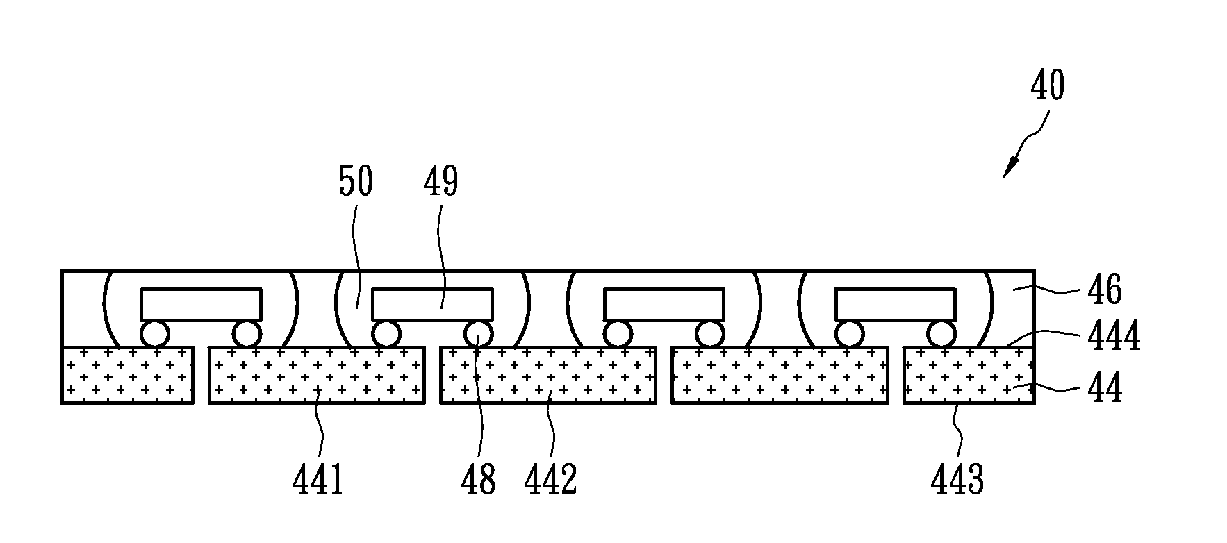
[0027]FIGS. 3A through 3E are schematic illustrations showing the manufacturing steps of the package module structure of compound semiconductor devices in accordance with the present invention, in which flip chip technology is employed.

[0028]In FIG. 3A, a temporary substrate 43 includes a first surface 431 and a second surface 432. In this drawing, the first surface 431 is an upper surface and the second surface 432 is a lower surface. The temporary substrate 43 may be made of a metallic material, a ceramic material or a polymer material. A heat dissipation film 44 with a pattern is formed on the first surface 431 through printing, screening, electroform, chemical plating (or electroless plating) or sputtering. In this embodiment, the heat dissipation film 44 is an electrically conductive film including an N-type electrode 441 and a P-type electrode 442, which are disposed at two sides of each isolation gap 70 to form required circuits of the package module structure. The electrical...


PUM


Abstract

A compound semiconductor device package module structure includes a heat dissipation film, a dielectric layer, a plurality of compound semiconductor dies, means for mounting the compound semiconductor dies on the heat dissipation film, and a transparent encapsulation material. The dielectric layer includes a plurality of openings formed on the heat dissipation film. The compound semiconductor dies are placed on the heat dissipation film in the openings, and adjacent two compound semiconductor dies are separated by the dielectric layer. The transparent encapsulation material covers the compound semiconductor dies.

Description

BACKGROUND OF THE INVENTION[0001](A) Field of the Invention[0002]The present invention relates to a package module structure of compound semiconductor devices and fabricating method thereof, and more particularly, to a thin package module structure for a photoelectric semiconductor device and fabricating method thereof.[0003](B) Description of the Related Art[0004]Because the light emitting diode (LED) pertaining to the photoelectric device has advantages of a small body, high efficiency and long lifetime, it is deemed as an excellent illuminant source for the next generation. Furthermore, LCD (liquid crystal display) technology is developing rapidly and full color is the current trend in electronic product displays. Therefore, the white series LEDs are not only applicable to indication lights and large size display screens but also to most consumer electronics products such as mobile phones and personal digital assistants (PDA).[0005]FIG. 1 is a schematic cross-sectional diagram of...

Claims


Application Information

Patent Timeline
Patent Type & Authority Applications(United States)
IPC IPC(8): H01L23/36H01L21/58
CPCH01L21/568H01L23/3135H01L24/16H01L24/48H01L24/93H01L2224/16245H01L2224/48247H01L2924/01078H01L2924/12044H01L2924/01087H01L33/52H01L2224/451H01L2224/73265H01L2924/00014H01L2924/12041H01L2924/181H01L2924/00H01L2224/05599H01L2924/00012H01L2224/45099H01L2224/45015H01L2924/207
Inventor TSENG, WEN LIANGCHEN, LUNG HSINKUO, CHESTER
Owner ADVANCED OPTOELECTRONICS TECH
Learn More