
Signal amplification circuit

a signal amplification circuit and signal amplification technology, applied in the direction of differential amplifiers, amplifiers with semiconductor devices/discharge tubes, negative-feedback circuit arrangements, etc., can solve the problem of inability to perform the original function of a pressure sensor, the range of variation of saturation voltage of a conventional signal amplification circuit, and the ecu misdiagnosis of the situation, etc. problem, to achieve the effect of increasing the sink/source capacity, increasing the current consumption, and reducing the current consumption problem

Active Publication Date: 2010-04-22
FUJI ELECTRIC CO LTD
View PDF2 Cites 5 Cited by
  • Summary
  • Abstract
  • Description
  • Claims
  • Application Information

AI Technical Summary

Benefits of technology

The present invention provides a low-current consumption type signal amplification circuit with stable operation and no large increases in current consumption due to the sink / source capacity of a negative feedback amplification circuit or the upper / lower limiting circuits. The circuit includes a negative feedback amplification circuit with first and second voltage limiting circuits, first and second reference voltage sources, and first and second op-amps. The first voltage limiting circuit increases the resistance of the output terminal of the negative feedback amplification circuit when the output voltage falls below the first reference voltage, while the second voltage limiting circuit increases the resistance of the output terminal when the output voltage rises above the second reference voltage. The negative feedback amplification circuit has a first PMOS transistor and a first NMOS transistor forming the output stage, and the first op-amp fixes the lower-limit saturation voltage of the negative feedback amplification circuit at the first reference voltage. The second op-amp fixes the upper-limit saturation voltage of the negative feedback amplification circuit at the second reference voltage. The negative feedback amplification circuit has a high-potential side of the power supply and a low-potential side of the power supply, and the first and second reference voltage sources provide the reference voltages for the first and second voltage limiting circuits. The first and second reference voltage sources have different reference voltages, and the first and second op-amps have different input terminals. The circuit provides a low-current consumption type signal amplification circuit with stable operation and no large increases in current consumption.

Problems solved by technology

However, due to the effect of the above-described “manufacturing variance” and “temperature dependence”, when the output voltage range of the signal amplification circuit 10c in FIG. 8 has become broad (does not readily reach saturation), the output voltage is as indicated by the dotted line a. The output characteristic of the dotted line a is such that the saturation voltage is positioned in a diagnostic region, so that even when the pressure sensor is in steady operation, cases occur in which the saturation voltage enters into a diagnostic region, and in this case the problem arises that the ECU misdiagnoses the situation as a “sensor malfunction”.
Conversely, when the output voltage range of the signal amplification circuit 10c in FIG. 8 becomes narrow (saturation easily occurs), the shape is as indicated by the dotted line c, and saturation occurs in the region in which a voltage which is linear with respect to pressure should be output (the region close to Vb and Vc), and there is the problem that the original function of a pressure sensor cannot be performed.
However, the range of variation of saturation voltage for a conventional signal amplification circuit 10c (in FIG. 8) is too broad to be absorbed.
The manufacturing variation can be decreased through measures taken in pressure sensor characteristic selection and manufacturing methods, but increases in manufacturing costs result.
On the other hand, temperature dependence is related to the temperature dependences specific to materials, and so is not easily reduced.
H7-209326, when it is necessary to increase the sink / source capacity of the negative feedback amplification circuit, for example in low-resistance load driving or similar, the current consumption increases dramatically.
And when the value of the upper-limit limiting voltage is low and the value of the lower-limit limiting voltage is high, current consumption increases dramatically.
The above are details of the collision state; due to this complexity, in the actual circuits unstable time periods tend to occur.

Method used


Image

  • Signal amplification circuit
  • Signal amplification circuit
  • Signal amplification circuit

Examples


embodiment 1

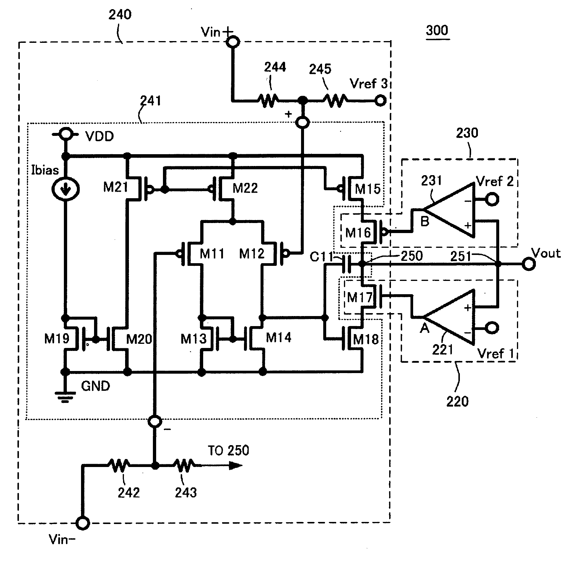
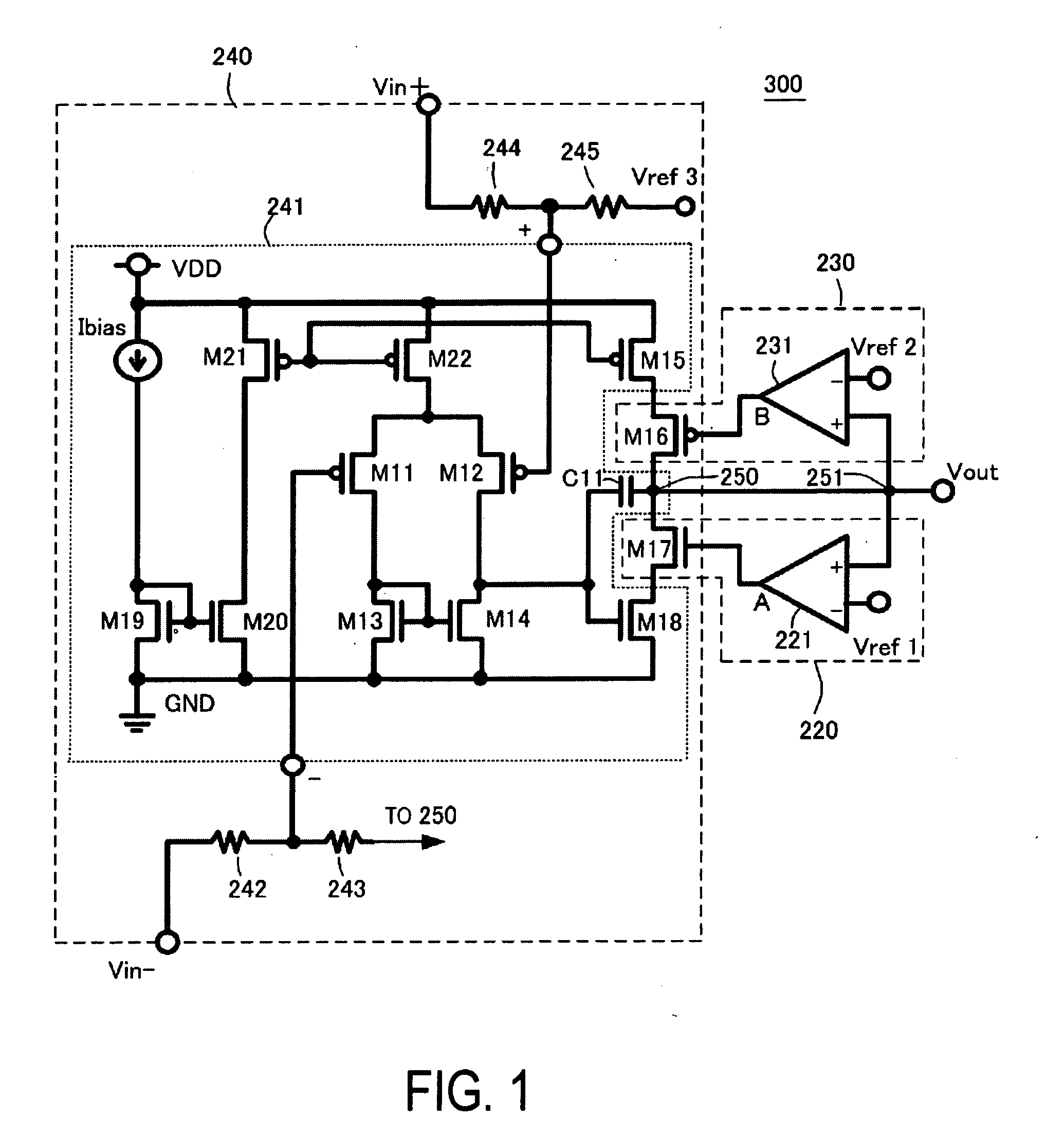
[0096]FIG. 1 is a circuit diagram of principal portions of the signal amplification circuit of a first embodiment of the invention. Below, the circuit configuration is explained.

[0097]The signal amplification circuit 300 comprises a negative feedback amplification circuit 240, upper-limit voltage limiting circuit 230, and lower-limit voltage limiting circuit 220. The negative feedback amplification circuit 240 comprises an op-amp 241 and resistors 242, 243, 244, 245; the resistor 242 is connected to the Vin-terminal (negative input terminal), the resistor 244 is connected to the Vin+terminal (positive input terminal), and the resistor 245 is connected to a third reference voltage Vref3. The upper-limit voltage limiting circuit 230 and lower-limit voltage limiting circuit 220 are respectively a second voltage limiting circuit and a first voltage limiting circuit.

[0098]The upper-limit voltage limiting circuit 230 comprises an op-amp 231 and M16; the lower-limit voltage limiting circui...

embodiment 2

[0129]FIG. 5 is a circuit diagram of principal portions of the signal amplification circuit of a second embodiment of the invention. The same elements as in FIG. 1 are denoted by the same numerals in FIG. 1. Differences from FIG. 1 include the fact that voltage division between VDD and ground is performed by the resistors R31 to R34, the connection point of R32 and R33 is connected to the Vout terminal, the connection point of R31 and R32 is connected to the +terminal of the op-amp 221, and the connection point of R33 and R34 is connected to the +terminal of the op-amp 231.

[0130]This signal amplification circuit 400 comprises a negative feedback amplification circuit 240, upper-limit voltage limiting circuit 230a, and lower-limit voltage limiting circuit 220a. The upper-limit voltage limiting circuit 230a comprises an op-amp 231, R33, R34, and M16; the lower-limit voltage limiting circuit 220a comprises an op-amp 221, R31, R32, and M17.

[0131]As explained above, R33 and R34 are serie...

embodiment 3

[0140]In the above embodiments, devices were described having both a lower-limit voltage limiting circuit and an upper-limit voltage limiting circuit; but a device may have only one of these circuits.

[0141]FIG. 16 and FIG. 17 are circuit diagrams of principal portions of signal amplification circuits of this invention.

[0142]FIG. 16A is the signal amplification circuit of FIG. 1, having only a lower-limit voltage limiting circuit, and FIG. 16B is the signal amplification circuit of FIG. 1, having only an upper-limit voltage limiting circuit. The same elements as in FIG. 1 are denoted by the same reference numerals as in FIG. 1.

[0143]FIG. 17A is the signal amplification circuit of FIG. 5, having only a lower-limit voltage limiting circuit, and FIG. 17B is the signal amplification circuit of FIG. 5, having only an upper-limit voltage limiting circuit. The same elements as in FIG. 5 are denoted by the same reference numerals as in FIG. 5.

[0144]In FIG. 16 and FIG. 17 also, the op-amp of ...


PUM


Abstract

This invention provides a low-current consumption type signal amplification circuit, which limits the output voltage to fix a lower-limit (upper-limit) saturation voltage of the amplification circuit at a predetermined lower-limit (upper-limit) limiting voltage. The signal amplification circuit comprises a negative feedback amplification circuit, a lower-limit voltage limiting circuit and an upper-limit voltage limiting circuit. The lower-limit voltage limiting circuit increases a resistance between an output terminal of the negative feedback amplification circuit and a ground terminal when the output voltage of the negative feedback amplification circuit falls below the lower-limit limiting voltage. The upper-limit voltage limiting circuit increases a resistance between the output terminal of the negative feedback amplification circuit and a high-potential side of a power supply when the output voltage of the negative feedback amplification circuit rises above the upper-limit limiting voltage.

Description

BACKGROUND OF THE INVENTION[0001]1. Field of the Invention[0002]This invention relates to a signal amplification circuit for electrical and electronic equipment, used in automobiles, two-wheeled motor vehicles, and in industry, and in particular relates to a signal amplification circuit of a semiconductor physical quantity sensor used in automobiles and two-wheeled motor vehicles.[0003]2. Description of the Related Art[0004]At present, in the fields of automobiles and two-wheeled motor vehicles, there is an accelerating move toward control by electrical and electronic components of portions that heretofore had been controlled by mechanical components.[0005]Moreover, electronic component products used in the past are becoming increasingly precise and multifunctional, aiming at more sophisticated control.[0006]For example, pressure sensors used to measure the pressure within an intake manifold or to measure brake hydraulic pressure are now required to have a function to detect their o...

Claims


Application Information

Patent Timeline
Patent Type & Authority Applications(United States)
IPC IPC(8): H03F1/34
CPCH03F3/45085H03F3/45179H03F3/45475H03F2203/45646H03F2200/261H03F2203/45418H03F2203/45424H03F3/45659
Inventor NISHIKAWA, MUTSUOUEMATSU, KATSUYUKIWATSUNAMI, KAZUHIRO
Owner FUJI ELECTRIC CO LTD
Learn More