Semiconductor light emitting device, and backlight and display device comprising the semiconductor light emitting device

a light emitting device and semiconductor technology, applied in semiconductor devices, instruments, electrical devices, etc., can solve the problems of harm to the environment, inferior leds in light intensity difference and brightness uniformity of emitted light to cold-cathode tubes, and non-uniformity of emitted light, so as to improve the uniformity of light emitted from wavelength converting materials, improve the emitted light color balance, and improve the effect of uniformity

Active Publication Date: 2010-04-29
SEOUL SEMICONDUCTOR
View PDF3 Cites 32 Cited by
  • Summary
  • Abstract
  • Description
  • Claims
  • Application Information

AI Technical Summary

Benefits of technology

[0018]In the semiconductor light emitting device according to the present invention, a light intensity difference reducing layer is provided between an ultraviolet semiconductor light emitting element and a wavelength converting material layer. Accordingly, light (including ultraviolet light and the like) produced in the ultraviolet semiconductor light emitting element is rendered uniform during passage through the light intensity difference reducing layer, and thus, uniform light reaches the wavelength converting material layer. Therefore, the uniformity of light emitted from the wavelength converting material can be improved.
[0019]The homogenization of light, which reaches the wavelength converting material layer, homogenizes the color of light emitted from a phosphor present in the wavelength converting material layer, and particularly improves an emitted light color balance of a plurality of types of phosphors present in the wavelength converting material layer. Accordingly, a multicolor light emitting device, which has good color rendering properties and can realize more natural color representation, can be provided.
[0020]Thus, the light emitting device according to the present invention can be utilized in various applications by utilizing its excellent properties. The light emitting device according to the present invention is particularly suitable for use, for example, as light emitting devices in various display devices, preferably, for example, in equipment where a reduction in size, a reduction in weight, a reduction in thickness, electric power saving, brightness high enough to realize good visibility even in sunlight, and good color rendering properties are particularly required, for example, cellular phones, personal digital assistants, electronic dictionaries, digital cameras, computers, liquid crystal televisions (TVs), and peripheral equipment of these devices.

Problems solved by technology

The cold-cathode tubes contain, for example, mercury and thus are harmful to an environment.
The LEDs, however, are inferior in the light intensity difference and brightness uniformity of emitted light to the cold-cathode tubes.
There are mainly three types of non-uniformity of emitted light which pose a problem associated with LEDs.
No matter how the LEDs are arrayed, a complete line light source or a surface light source cannot be provided.
This poses a problem that non-uniformity of brightness occurs due to the presence of a part where a bright light is emitted by LEDs, and a non-light emitting part present between the LED and the other LED.
The color uniformity is a problem involved in a combination of LED with a wavelength converting material such as a phosphor material to emitt, for example, white light.
This technique, however, is disadvantageous in that, when the emitted light is viewed in a certain direction, the emitted light is seen as a yellowish color, and nonuniform yellow and blue colors appear upon projection on a white surface.
On the other hand, any effective measure for eliminating the problem of non-uniformity of the emitted light has not been proposed, and the problem of non-uniformity of the emitted light has been a big problem.

Method used


Image

  • Semiconductor light emitting device, and backlight and display device comprising the semiconductor light emitting device
  • Semiconductor light emitting device, and backlight and display device comprising the semiconductor light emitting device
  • Semiconductor light emitting device, and backlight and display device comprising the semiconductor light emitting device

Examples


example 1

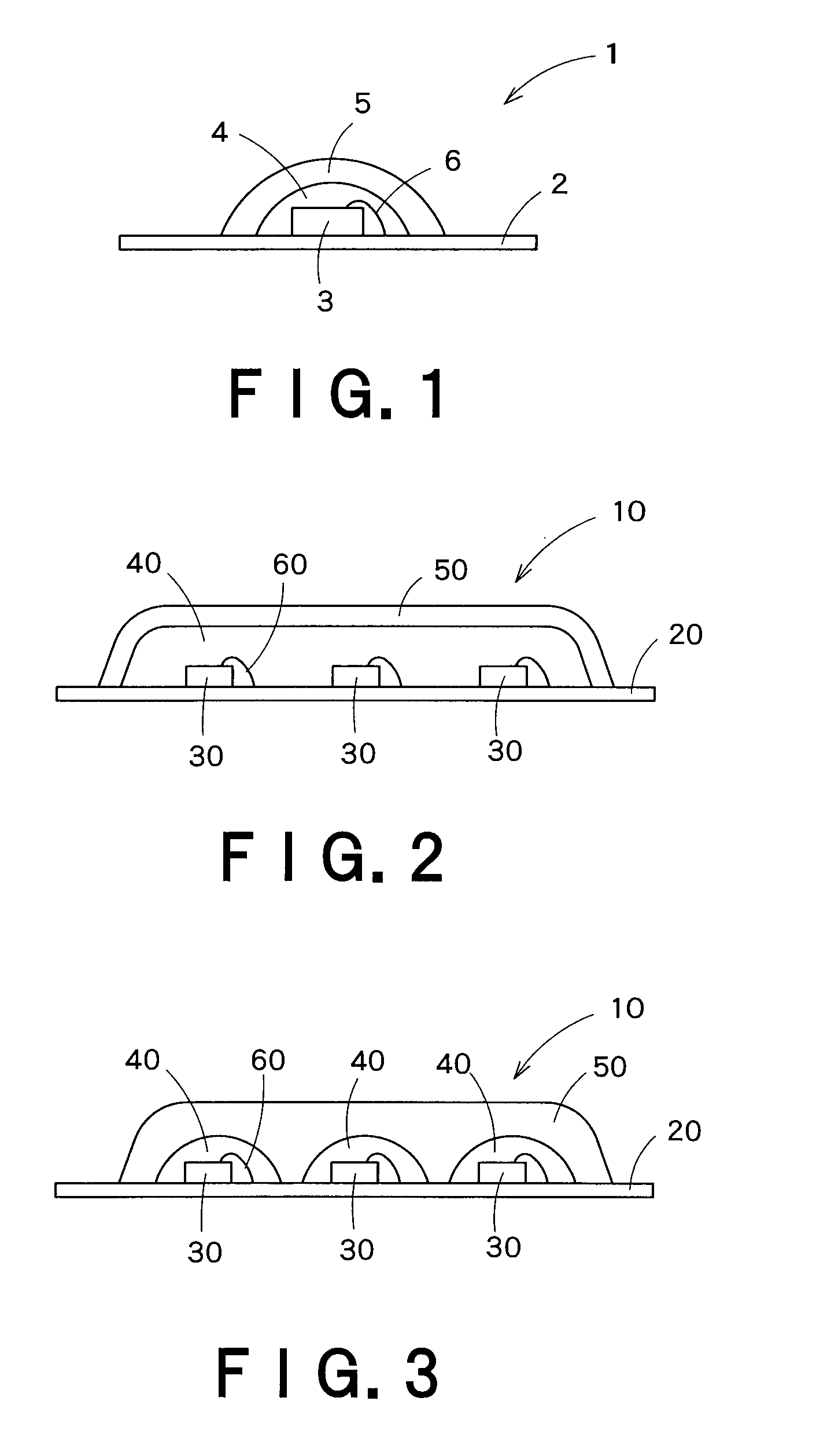
[0082]The semiconductor light emitting device according to the present invention shown in FIG. 1 was produced by the following process.

[0083]An ultraviolet emitting light emitting diode (LED) was die bonded to a substrate (2.0 mm in length×2.0 mm in width) with a wiring pattern electrode by using a solder paste or the like. The bonded LED chip was wire bonded with a gold wire to a wiring pattern. After the confirmation of lighting of the ultraviolet emitting LED, the ultraviolet emitting LED and the gold wire were covered with a heat curable transparent silicone resin. In covering the LED and the gold wire, a necessary amount of the silicone resin was coated by a dispenser, a mask or the like so that, after coating, the ultraviolet emitting LED was located at the center part. Thereafter, the coating was heat cured at a temperature of 100 to 150° C., and, if necessary, the procedure consisting of coating and heat curing was repeated, whereby a light intensity difference reducing laye...

example 2

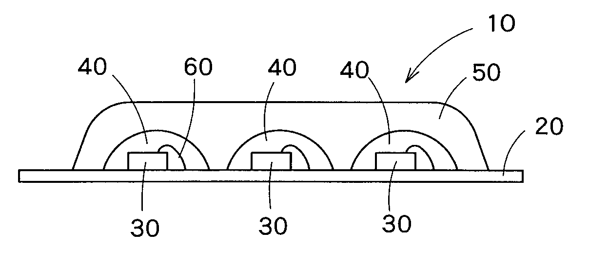
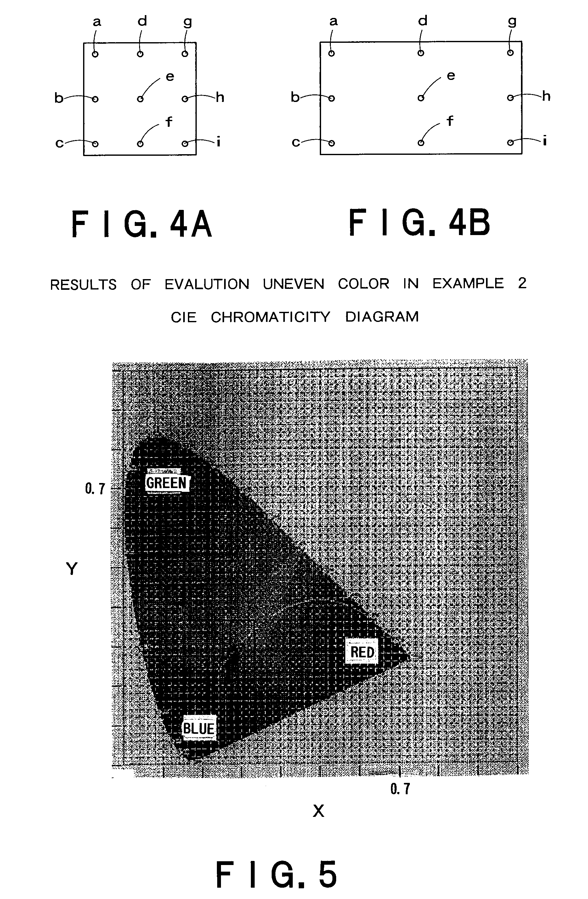
[0086]A semiconductor light emitting device according to the present invention shown in FIG. 2 was produced by the following process.

[0087]Three ultraviolet emitting LEDs were die bonded to a substrate (8.0 mm in length×3.0 mm in width) with a wiring pattern electrode by using a solder paste or the like at intervals of 2.0 mm. The bonded LED chips were wire bonded with a gold wire to a wiring pattern. After the confirmation of lighting of the ultraviolet emitting LEDs, the ultraviolet emitting LEDs and the gold wires were covered with a heat curable transparent silicone resin. In covering the LEDs and the gold wires, a necessary amount of the silicone resin was coated by a dispenser, a mask or the like so that, after coating, the central ultraviolet emitting LED was located at the center part, and the three ultraviolet emitting LEDs were covered with a continuous light intensity difference reducing layer common to the three LEDs. Thereafter, the coating was heat cured at a temperatu...

example 3

[0090]A semiconductor light emitting device according to the present invention shown in FIG. 3 was produced by the following process.

[0091]Three ultraviolet emitting LEDs were die bonded to a substrate (8.0 mm in length×3.0 mm in width) with a wiring pattern electrode by using a solder paste or the like at intervals of 2.0 mm. The bonded LED chips were wire bonded with a gold wire to a wiring pattern. After the confirmation of lighting of the ultraviolet emitting LEDs, the ultraviolet emitting LEDs and the gold wires were covered with a heat curable transparent silicone resin. In covering the LEDs and the gold wires, a necessary amount of the heat curable transparent silicone resin was coated by a dispenser, a mask or the like so that, after coating, the central ultraviolet emitting LED was located at the center part, and the three ultraviolet emitting LEDs were included in respective separate independent light intensity difference reducing layers. Thereafter, the coatings were heat...


PUM


Abstract

The present invention provides a semiconductor light emitting device comprising a light intensity difference reducing layer provided between an ultraviolet semiconductor light emitting element and a wavelength converting material layer, and a backlight and a display device comprising the semiconductor light emitting device. The semiconductor light emitting device is an LED light emitting device which has improved uniformity of emitted light and reduced non-uniformity of brightness and chromaticity of emitted light. The light emitting device according to the present invention is particularly suitable for use in various display devices, preferably, for example, in display devices in equipment where a reduction in size, a reduction in weight, a reduction in thickness, electric power saving, high brightness, and excellent color rendering properties are particularly required, for example, cellular phones, personal digital assistants, electronic dictionaries, digital cameras, computers, liquid crystal televisions (TVs), and peripheral devices of these devices.

Description

TECHNICAL FIELD[0001]The present invention relates to a semiconductor light emitting device, and a backlight and a display device using the semiconductor light emitting device. More particularly, the present invention relates to a semiconductor light emitting device having no significant nonuniform brightness and color of emitted light and a backlight and a display device using the semiconductor light emitting device.BACKGROUND ART[0002]Light emitting diodes (hereinafter referred to as “LEDs”) are semiconductor elements that convert electric energy to light such as ultraviolet light or visible light which is then radiated. An LED lamp comprising a chip of the LED sealed, for example, with a transparent resin is used in various fields. The LED chip is a semiconductor element and thus has a prolonged service life, is highly reliable, and, when used as a light source, can reduce replacement work and the like. Accordingly, the LED chip is becoming widely used as components constituting ...

Claims


Application Information

Patent Timeline
Patent Type & Authority Applications(United States)
IPC IPC(8): H01L33/00H01L33/50H01L33/52
CPCG02F1/133603G02F1/133609H01L33/52H01L33/507G02F2001/133614H01L2924/181H01L2224/48091H01L2224/45144G02F1/133614H01L25/0753H01L2924/00012H01L2924/00014H01L2924/00
Inventor OOYA, YASUMASASAKAI, RYOTAKEUCHI, HAJIMEISHII, TSUTOMI
Owner SEOUL SEMICONDUCTOR
Why Eureka
Try Eureka