Integrated Infrared and Color CMOS Imager Sensor

a color and infrared technology, applied in the field of cmos imagers, can solve the problems of high noise and image lag of devices, impracticality of using 4t aps, and high noise of devices, and achieve the effect of low reset noise and low leakage curren

Active Publication Date: 2010-04-29
SMARTSENS TECH (SHANGHAI) CO LTD
View PDF14 Cites 90 Cited by
  • Summary
  • Abstract
  • Description
  • Claims
  • Application Information

AI Technical Summary

Benefits of technology

[0014]Described herein is a CMOS imager structure that can detect IR and visible light. The device does not required vertically integrated photodiodes, as both the IR pixel and visible light detection pixels use a 4T buried photodiode. APS. Therefore, low leakage current, low reset noise, and complete charge transfer are possible.

Problems solved by technology

However, the use of a 4T APS is impractical, as the bottom photodiode for the IR detection is so deep that a complete charge transfer is almost impossible.
If the 4T APS is used for the IR detection, the device has a high noise and image lag resulting from incomplete charge transfer.
The design could be enabled using a 3T APS, however, such a CMOS imager is widely known to suffer from high circuit noise and high dark current.

Method used


Image

  • Integrated Infrared and Color CMOS Imager Sensor
  • Integrated Infrared and Color CMOS Imager Sensor
  • Integrated Infrared and Color CMOS Imager Sensor

Examples


Embodiment Construction

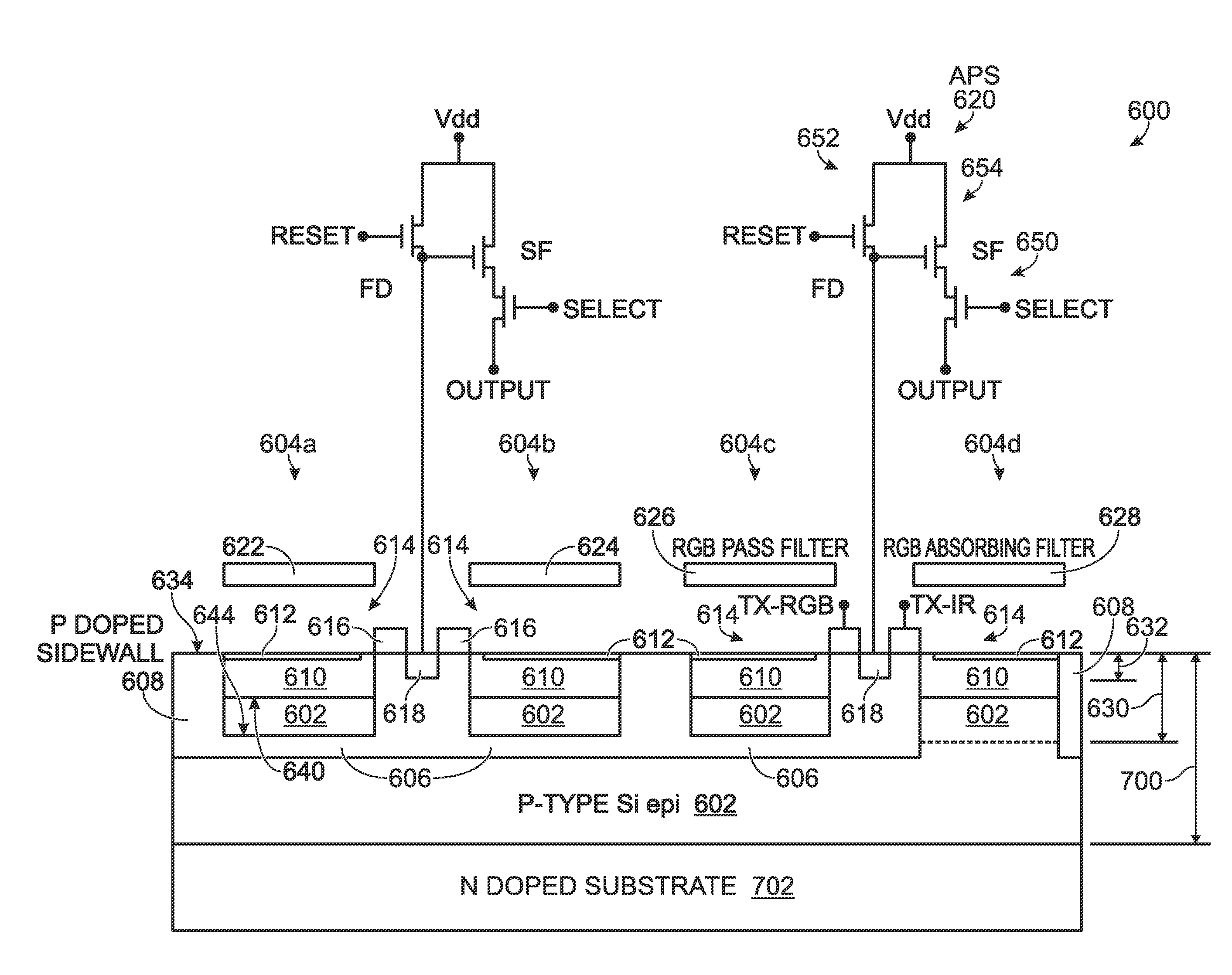
[0027]FIG. 6 is a partial cross-sectional view of an integrated IR and full color complementary metal oxide semiconductor (CMOS) imager array. The array 600 comprises a lightly doped p doped silicon (Si) substrate 602 and a plurality of pixel cells. Each pixel cell includes at least one visible light detection pixel. Shown are three visible light detection pixels 604a, 604b, and 604c. In other aspect, see FIG. 9B, each IR with more than three visible light detection pixels. In other words, there is no limitation to the number of visible light, detection pixels that may be associated with an IR pixel.

[0028]Each visible light pixel 604 includes a moderately p doped bowl with a bottom p doped layer 606 and p doped sidewalls 608. An n doped layer 610 is enclosed by the p doped bowl. A moderately p doped surface region 612 overlies the n doped layer 610. A transfer transistor 614 has a gate electrode 616 overlying the p doped sidewalk 608, a source formed from the n doped layer 610, and ...


PUM


Abstract

An integrated infrared (IR) and full color complementary metal oxide semiconductor (CMOS) imager array is provided. The array is built upon a lightly doped p doped silicon (Si) substrate. Each pixel cell includes at least one visible light detection pixel and an IR pixel. Each visible light pixel includes a moderately p doped bowl with a bottom p doped layer and p doped sidewalls. An n doped layer is enclosed by the p doped bowl, and a moderately p doped surface region overlies the n doped layer. A transfer transistor has a gate electrode overlying the p doped sidewalls, a source formed from the n doped layer, and an n+ doped drain connected to a floating diffusion region. The IR pixel is the same, except that there is no bottom p doped layer. An optical wavelength filter overlies the visible light and IR pixels.

Description

BACKGROUND OF THE INVENTION[0001]1. Field of the Invention[0002]This invention generally relates to integrated circuit (IC) fabrication and, more particularly, a CMOS imager capable of detecting both visible light and near infrared (IR), and an associated fabrication process.[0003]2. Description of the Related Art[0004]FIG. 1 depicts a complementary metal oxide semiconductor (CMOS) imager with a “buried” or “pinned” photodiode and a four-transistor (4T) active pixel sensor (APS) (prior art). Conventionally, the image cell, circuit includes four transistors and one photodiode. The pixel operation is divided into three main stages: reset, exposure, and reading.[0005](1) The reset stage: by turning on the reset and transfer (Tx) transistors, the photodiode capacitance is charged to a reset voltage. As for the case of the p+np buried photodiode shown in FIG. 1, the buried cathode (n) is totally depleted and set to the pinned voltage (Vpin).[0006](2) The exposure stage: with the absorpti...

Claims


Application Information

Patent Timeline
Patent Type & Authority Applications(United States)
IPC IPC(8): H01L31/112H01L31/18
CPCH01L27/14609H01L27/14645H01L27/1463H01L27/14621
Inventor LEE, JONG-JANTWEET, DOUGLAS J.SPEIGLE, JON M.
Owner SMARTSENS TECH (SHANGHAI) CO LTD
Why Eureka
Try Eureka