Wideband strip fed patch antenna

a patch antenna and wideband strip technology, applied in the direction of elongated active element feed, resonant antenna, radiating element structure, etc., can solve the problems of affecting the bandwidth, affecting the scan angle and cross polarization, disadvantageously increasing the size of the antenna, etc., to reduce cross polarized radiation, wideband antenna operation, and improved bandwidth

Inactive Publication Date: 2010-04-29
LOCKHEED MARTIN CORP
View PDF21 Cites 45 Cited by
  • Summary
  • Abstract
  • Description
  • Claims
  • Application Information

AI Technical Summary

Benefits of technology

[0012]The strips are electrically excited 180 degrees out-of-phase to reduce cross-polarized radiation. By manipulating the associated strip and an associated electrical connector inductance and capacitance, the electric fields are favorably disposed to achieve wideband antenna operation. This bandwidth can be improved further when dielectric loading is added to the portion between the strip and the first conductive element.
[0013]The present invention provides for a flexible, bendable, lightweight microstrip patch antenna with wide operational bandwidth (>20%) and low cross-polarized radiation (<−20dB) capable of operating in single or dual linear and / or single or dual circular polarization mode.

Problems solved by technology

Patch antenna radiating elements utilized for radar antenna arrays are inherently limited in bandwidth, scan angle and cross polarization.
In addition to bandwidth limitations, a patch design must take into consideration several trade-offs that affect size, weight, the effects of cross polarization, excitation of surface waves and current density, sensitivity and transmission and reception angle, and power.
These properties, among other things, affect the bandwidth.
However, increasing permittivity may in turn excite surface waves that contribute to scan blindness.
Increasing the dielectric substrate height for a back-fed patch antenna can increase operational bandwidth up to 25%, but will also disadvantageously increase the size of the antenna.
Such approach is limited by increasing inductance of the feed probe, which limits the substrate thickness and possible bandwidth increase.
However, these antennas tend to be extremely sensitive to probe dimensions and position.
Furthermore, cross polarized radiation remains a problem.
Using a dual probe feed 180° out-of-phase tends to reduce the high cross-polarization, but does not improve the operational bandwidth.

Method used


Image

  • Wideband strip fed patch antenna
  • Wideband strip fed patch antenna
  • Wideband strip fed patch antenna

Examples


Embodiment Construction

[0028]The following description of the preferred embodiments is merely by way of example and is in no way intended to limit the invention, its applications, or uses.

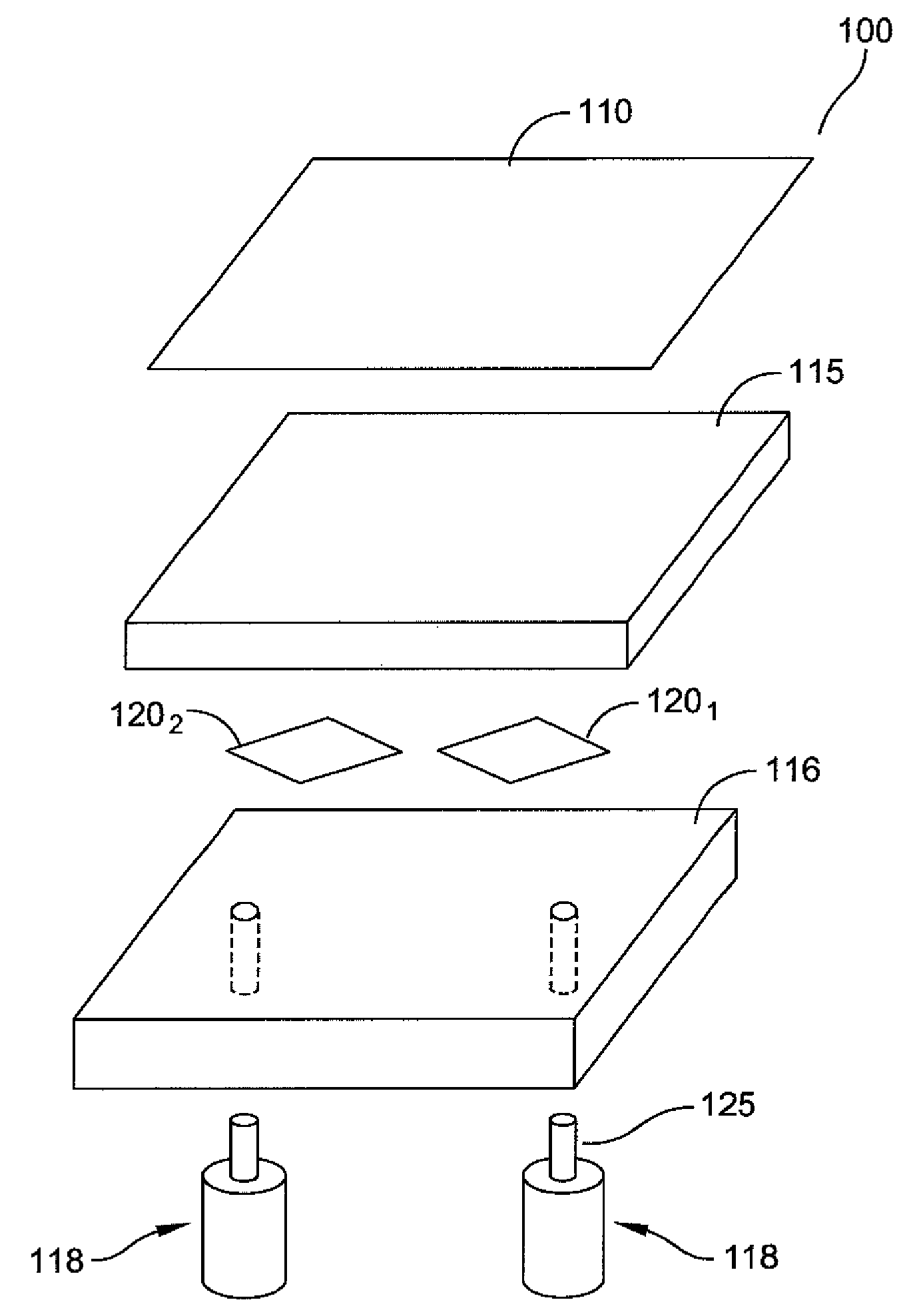
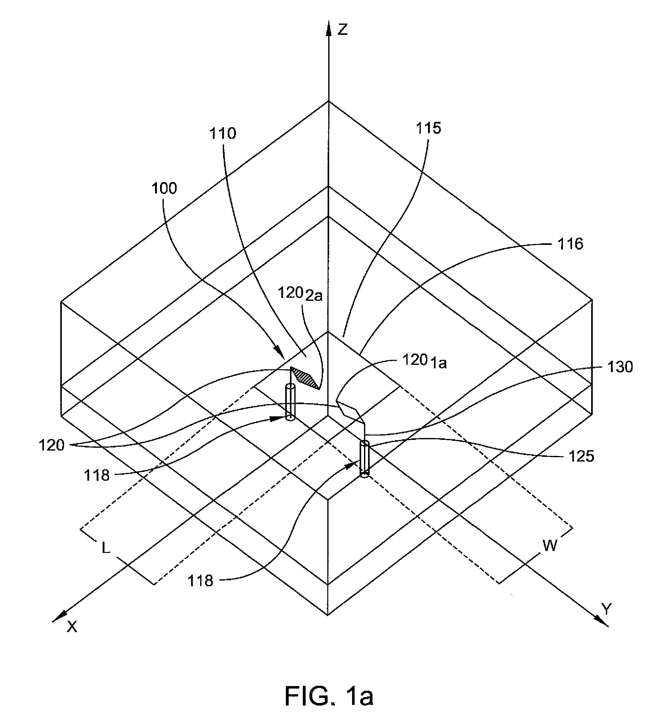
[0029]As shown in FIG. 1a, one embodiment of the invention relates to a microstrip patch antenna 100 that includes a patch antenna element comprising a conductive layer 110 and a pair of dual probe feeds 118 separate from one another and spaced from and field coupled to patch antenna element conductive layer 110 for transmitting or receiving RF signals. Each of the probe feeds 118 includes a vertically extending conductor segment 125 and a deltoid shaped conductive strip 120 orthogonal to the conductor segment 125. The deltoid shaped conductive strips (labeled generally as 120) are coplanar. A first dielectric layer 115 separates antenna element conductive layer 110 and the coplanar deltoid shaped conductive strips 120. As shown, each of the deltoid shaped conductive strips have their major surfaces extending toward one ...


PUM


Abstract

A microstrip patch antenna comprises a patch antenna element comprising a first conductive layer; dual probe feeds separate from each other and spaced from and field coupled to the patch antenna element for transmitting or receiving RF signals, each of the dual probe feeds having a conductor segment and a deltoid shaped conductive strip orthogonal to the conductor segment; the deltoid shaped conductive strips being coplanar; and a first dielectric material layer separating the first conductive layer and the coplanar deltoid shaped conductive strips.

Description

FIELD OF THE INVENTION[0001]The present invention relates to the field of antennas such as those used in phased array radar applications.BACKGROUND OF THE INVENTION[0002]Patch microstrip antennas are small, low-profile, low radar cross-section (RCS) and lightweight radiators ideal for phased array applications. In addition, a microstrip patch antenna is relatively inexpensive and easily manufactured, rugged, readily conformable to mount to an irregular shape, having a broad reception pattern, and can be adapted to receive multiple frequencies through proper configuration of the patches. Patch antenna radiating elements utilized for radar antenna arrays are inherently limited in bandwidth, scan angle and cross polarization. For example, a simple back-fed patch typically has a bandwidth of about 3% to about 7% of the operating center frequency. In addition to bandwidth limitations, a patch design must take into consideration several trade-offs that affect size, weight, the effects of ...

Claims


Application Information

Patent Timeline
Patent Type & Authority Applications(United States)
IPC IPC(8): H01Q1/38H01Q1/50H01Q21/00
CPCH01Q9/0457H01Q25/02H01Q21/065
Inventor TABAKOVIC, HARIS
Owner LOCKHEED MARTIN CORP
Why Eureka
Try Eureka