Dye-sensitized photoelectric conversion element module and a method of manufacturing the same, and electronic apparatus

a technology of photoelectric conversion element and dye sensitization, which is applied in the direction of cell components, final product manufacturing, sustainable manufacturing/processing, etc., can solve the problems of unsuitable thinning and weight saving of dye sensitized solar cell modules having z-type structures, and the inability to prevent dye adsorption to the counter electrode in terms of structure, so as to achieve no deterioration of characteristics and save weigh

Inactive Publication Date: 2010-05-06
SONY CORP
View PDF20 Cites 34 Cited by
  • Summary
  • Abstract
  • Description
  • Claims
  • Application Information

AI Technical Summary

Benefits of technology

[0010]However, the dye-sensitized solar cell module having the Z type structure was unsuitable for thinning and weight saving because it was necessary to use the two sheets of substrates. A dye-sensitized solar cell module having a monolithic structure which can be manufactured with one sheet of substrate is known. However, the dye-sensitized solar cell module having the monolithic structure has a demerit of being inferior to the dye-sensitized solar cell module having the Z type structure in a phase of the characteristics because there are a lot of limits to a material for a counter electrode, and also it is impossible to prevent dye adsorption to the counter electrode in terms of the structure.
[0011]In the light of the foregoing, a problem to be solved by the present invention is to provide a dye-sensitized photoelectric conversion element module such as a dye-sensitized solar cell in which only one sheet of substrate is required to be used, a counter electrode can be structured in a thin form, thereby making thinning and weight saving possible, and there is no restriction in a phase of a material for the counter electrode, and also which has the same performance of generation of electric power that of the dye-sensitized solar cell module having the Z type structure and a method of manufacturing the same, and an electronic apparatus using the excellent dye-sensitized photoelectric conversion element module described above.

Problems solved by technology

However, the dye-sensitized solar cell module having the Z type structure was unsuitable for thinning and weight saving because it was necessary to use the two sheets of substrates.
However, the dye-sensitized solar cell module having the monolithic structure has a demerit of being inferior to the dye-sensitized solar cell module having the Z type structure in a phase of the characteristics because there are a lot of limits to a material for a counter electrode, and also it is impossible to prevent dye adsorption to the counter electrode in terms of the structure.

Method used


Image

  • Dye-sensitized photoelectric conversion element module and a method of manufacturing the same, and electronic apparatus
  • Dye-sensitized photoelectric conversion element module and a method of manufacturing the same, and electronic apparatus
  • Dye-sensitized photoelectric conversion element module and a method of manufacturing the same, and electronic apparatus

Examples


example 1

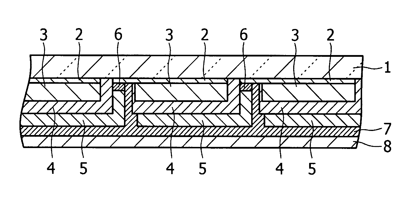
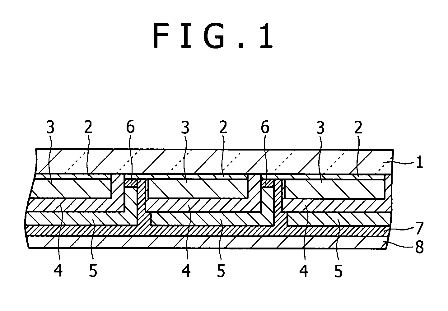
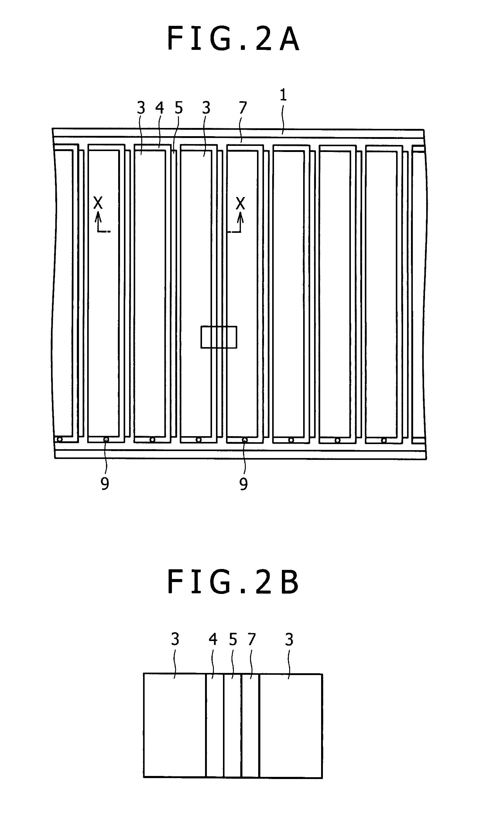
[0074]After an FTO film was formed on a glass substrate, the FTO film was patterned by etching to eight stripe-shaped patterns so as to define a gap, having a width of 0.5 mm, between each two stripe-shaped patterns. After that, ultrasonic cleaning was carried out by using acetone, alcohol, an alkali system cleaning liquid, and ultrapure water in order, and drying was sufficiently carried out.

[0075]A titanium oxide paste made by Solaronix was applied onto the glass substrate so as to obtain eight-shaped patterns (a total area was 16 cm2) each having a width of 5 mm, and a length of 40 mm by using a screen printer. With regard to the paste, a transparent Ti-Nanoxide TSP paste, and a Ti-Nanoxide DSP containing therein scattering particles were laminated in order from the glass substrate side so as to have a thickness of 7 μm, and a thickness of 13 μm, respectively. As a result, a porous TiO2 film having a thickness of 20 μm in total was obtained. After the porous TiO2 film was burnt i...

example 2

[0084]A dye-sensitized photoelectric conversion element module was manufactured similarly to the case of Example 1 except that a counter electrode was formed into a foil shape with a carbon paste.

example 3

[0085]A dye-sensitized photoelectric conversion element module was manufactured similarly to the case of Example 1 except that a counter electrode was formed into a foil shape with a platinum-supported carbon paste.


PUM

PropertyMeasurementUnit
melting pointaaaaaaaaaa
thicknessaaaaaaaaaa
particle diameteraaaaaaaaaa

Abstract

A dye-sensitized photoelectric conversion device is formed by sequentially arranging a dye-sensitized semiconductor layer (3), a porous insulating layer (4) and a counter electrode (5) on a transparent conductive layer (2) which is formed on a transparent substrate (1). The counter electrode (5) is composed of a metal or alloy foil having a catalyst layer on one surface which is on the porous insulating layer (4) side, or a foil made of a material having a catalytic activity. At a position between two adjacent dye-sensitized photoelectric conversion devices, the transparent conductive layer (2) of one dye-sensitized photoelectric conversion device and the counter electrode (5) of the other dye-sensitized photoelectric conversion device are electrically connected with each other. The dye-sensitized semiconductor layer (3) and the porous insulating layer (4) are impregnated with an electrolyte. Each dye-sensitized photoelectric conversion device is covered with a sealing layer (7).

Description

TECHNICAL FIELD[0001]The present invention relates to a dye-sensitized photoelectric conversion element module and a method of manufacturing the same, and an electronic apparatus, and, for example, is suitable for being applied to a dye-sensitized solar cell module using a dye-sensitized semiconductor layer made of semiconductor fine particles supporting a dye, and various kinds of electronic apparatuses.BACKGROUND ART[0002]It is said that when fossil fuel such as coal or oil is used as an energy source, the global warning is caused because carbon dioxide is generated due to use of the fossil fuel. In addition, use of a nuclear energy is fraught with a risk of contamination due to nuclear radiation. At present when many people talk about the environmental concerns, dependency on these energies is fraught with problems.[0003]On the other hand, the solar cell as a photoelectric conversion element for converting a solar light into an electrical energy exerts an extremely less influence...

Claims


Application Information

Patent Timeline
Patent Type & Authority Applications(United States)
IPC IPC(8): H01L31/0248H01L31/18H01L31/04H01M50/528
CPCH01G9/2013H01G9/2022H01G9/2031H01G9/2059H01G9/2081H01M4/9041H01M14/005Y02E10/542Y02T10/7022Y02P70/521Y02P70/50Y02T10/70Y02E60/50H01L31/042
Inventor MOROOKA, MASAHIROSUZUKI, YUSUKEYONEYA, REIKO
Owner SONY CORP
Why Eureka
Try Eureka