Semiconductor device
- Summary
- Abstract
- Description
- Claims
- Application Information
AI Technical Summary
Benefits of technology
Problems solved by technology
Method used
Image

Examples
first embodiment
[0035](Structure)
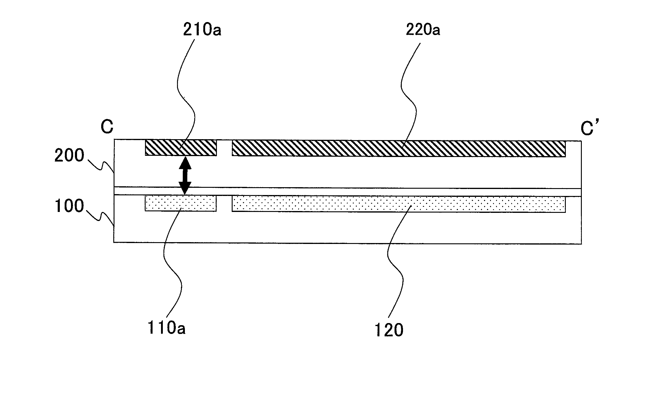
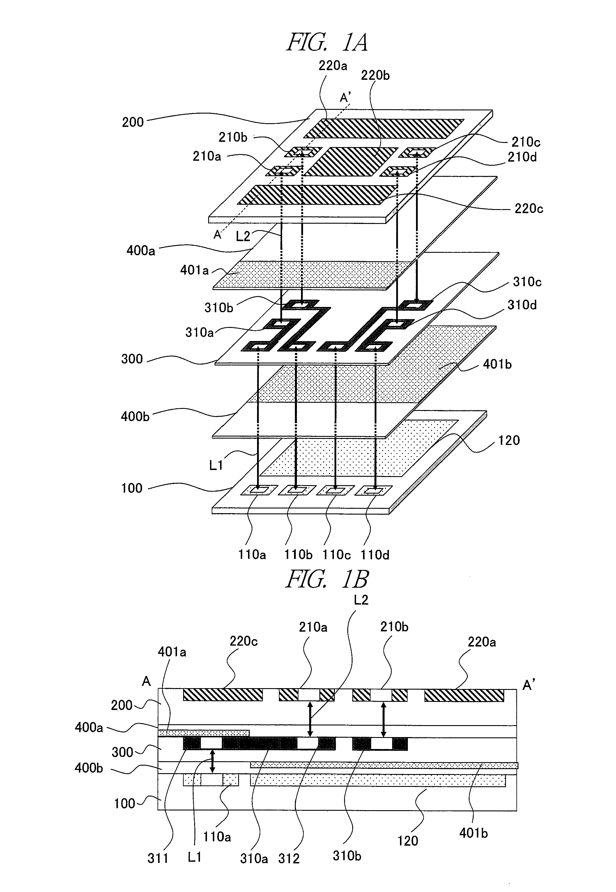
[0036]FIG. 1A is a perspective view illustrating a schematic configuration of an example of a semiconductor device according to a first embodiment of the present invention, and FIG. 1B is a cross-sectional view of the semiconductor device according to the present invention cut in a direction along the line A-A′ in FIG. 1A.
[0037]The semiconductor device according to the present embodiment has a transmitter LSI chip 100, a receiver LSI chip 200, an interposer 300, a first electromagnetic shield film 400a, and a second electromagnetic shield film 400b, which are stacked.
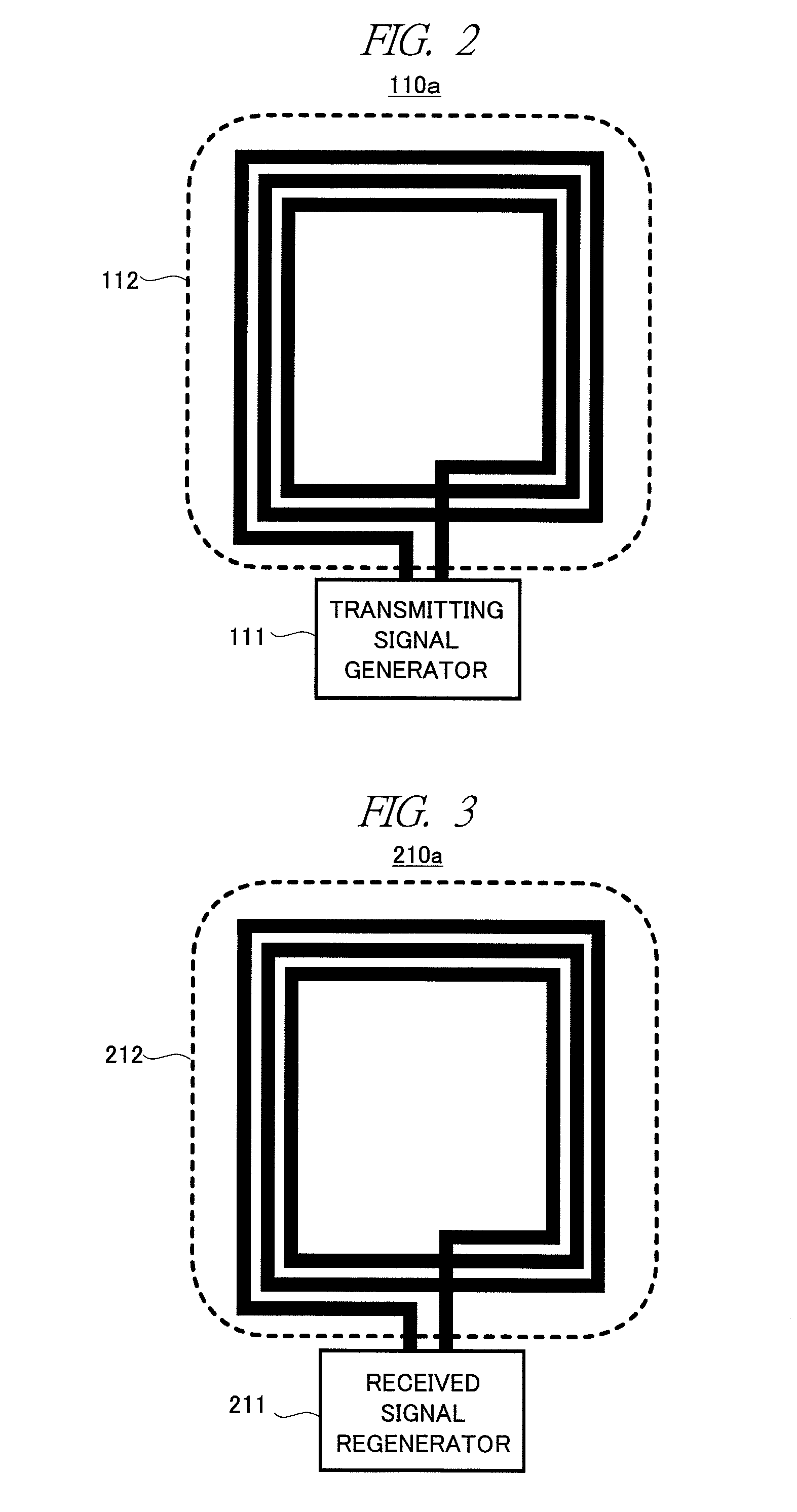
[0038]Transmitter circuits 110a to 110d and a processing unit of transmission data 120 are arranged on a surface of the transmitter LSI chip 100. The processing unit of transmission data 120 inputs data to the transmitter circuits 110a to 110d. Receiver circuits 210a to 210d and processing units of received data 220a to 220c are arranged on a surface of the receiver LSI chip 200. The processing units of...
second embodiment
[0075]FIG. 8 is a schematic diagram illustrating a schematic configuration of a semiconductor device according to a second embodiment of the present invention, and is a diagram compared to FIG. 1.
[0076]In reference to the semiconductor device in FIG. 8, a point different from the semiconductor device illustrated in FIG. 1 lies in that a transmission relay block 320 performs communication with the receiver circuits 210b and 210c. In this manner, signals transmitted from the transmitter circuit 110b can be transferred to the receiver circuits 210b and 210c. Note that parts corresponds to those in FIG. 1 are denoted by the same symbols in FIG. 8, and thus repetitive descriptions thereof will be omitted.
[0077]FIG. 9 is a schematic diagram illustrating an example of a planar configuration of the transmission relay block 320 according to the present embodiment. The transmission relay block 320 is composed of a first coil 321, second coils 322b and 322c, and a wiring connecting these three...
third embodiment
[0080]FIG. 11 is a diagram illustrating a planar configuration of a transmission relay block 340 according to a third embodiment of the present invention, and is compared with FIG. 4. In reference to the transmission relay block 340 of FIG. 11, a point different from the transmission relay block 310 illustrated in FIG. 4 lies in that the wire blocks 313a and 313b are substituted by a signal amplifier 341.
[0081]In the transmission relay block 340, the signal amplifier 341 operates to amplify signals, the signals being superimposed with the induced electromotive force generated at the first coil 311, upon transferring the signals to the second coil 312. A configuration example of a method of achieving the signal amplifier 341 is illustrated in FIG. 12.
[0082]In FIG. 12, passive devices 342a to 342f such as a resistive device, a capacitive device, and an inductive device are connected in a ladder-like form, so that a transfer path having a resonant characteristic to a predetermined freq...
PUM
 Abstract
Description
Claims
Application Information
 - Generate Ideas
- Intellectual Property
- Life Sciences
- Materials
- Tech Scout
- Unparalleled Data Quality
- Higher Quality Content
- 60% Fewer Hallucinations
Browse by: Latest US Patents, China's latest patents, Technical Efficacy Thesaurus, Application Domain, Technology Topic, Popular Technical Reports.
© 2025 PatSnap. All rights reserved.Legal|Privacy policy|Modern Slavery Act Transparency Statement|Sitemap|About US| Contact US: help@patsnap.com