Semiconductor memory device

Inactive Publication Date: 2010-05-06
RAMBUS INC
View PDF9 Cites 8 Cited by
  • Summary
  • Abstract
  • Description
  • Claims
  • Application Information

AI Technical Summary

Benefits of technology

[0015]The present invention enhances the random access capabilities to memory banks as well as enables high-speed writing and reading of data.
[0016]FIG. 1 is a view showing the configuration of the semiconductor memory device in which the present invention is implemented.
[0017]FIG. 2 is a view showing the detailed configuration of the data control circuit.
[0018]FIG. 3 is a view showing the

Problems solved by technology

However, in spite of above-mentioned strengths, the

Method used


Image

  • Semiconductor memory device
  • Semiconductor memory device
  • Semiconductor memory device

Examples


first embodiment

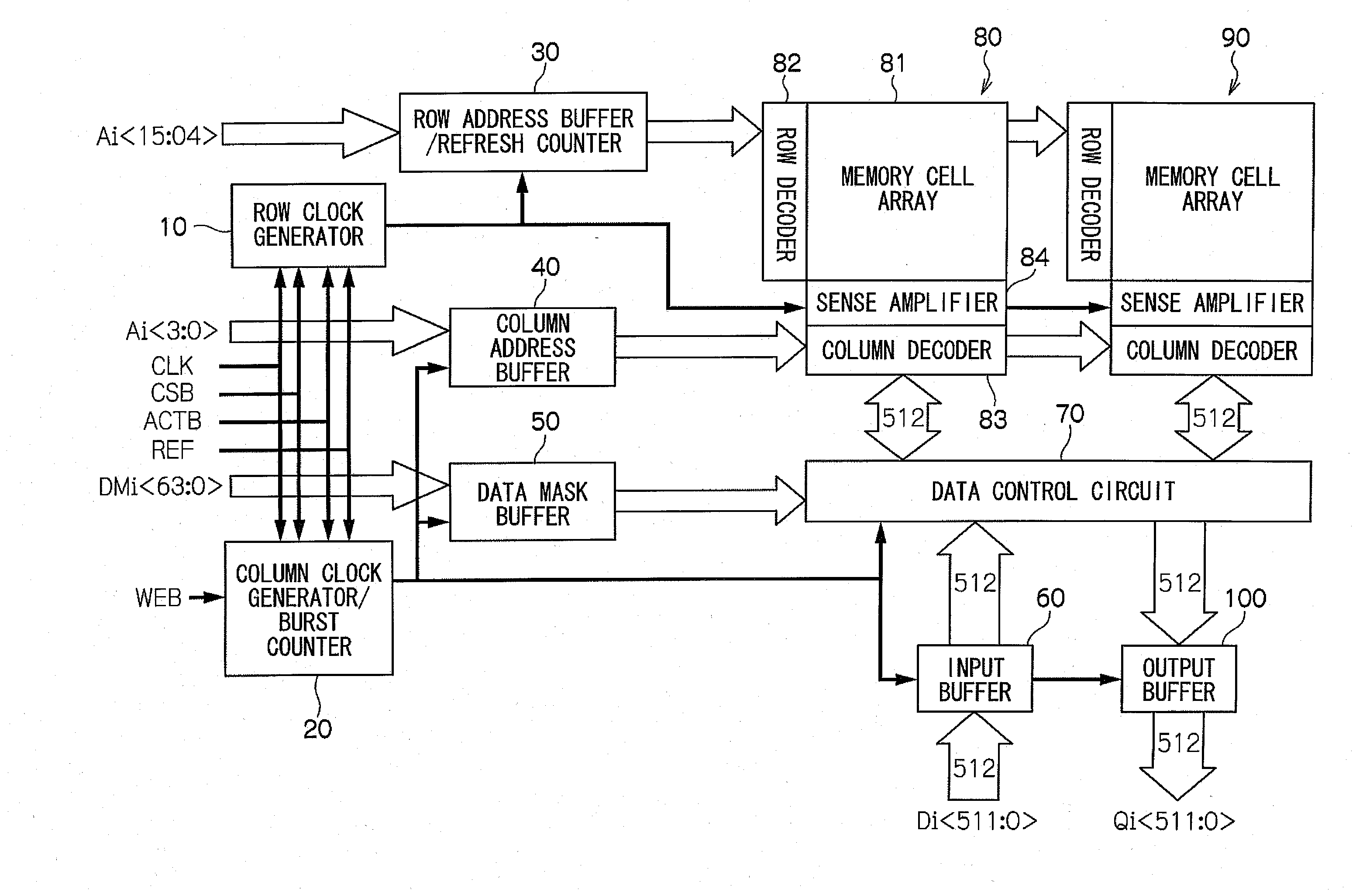
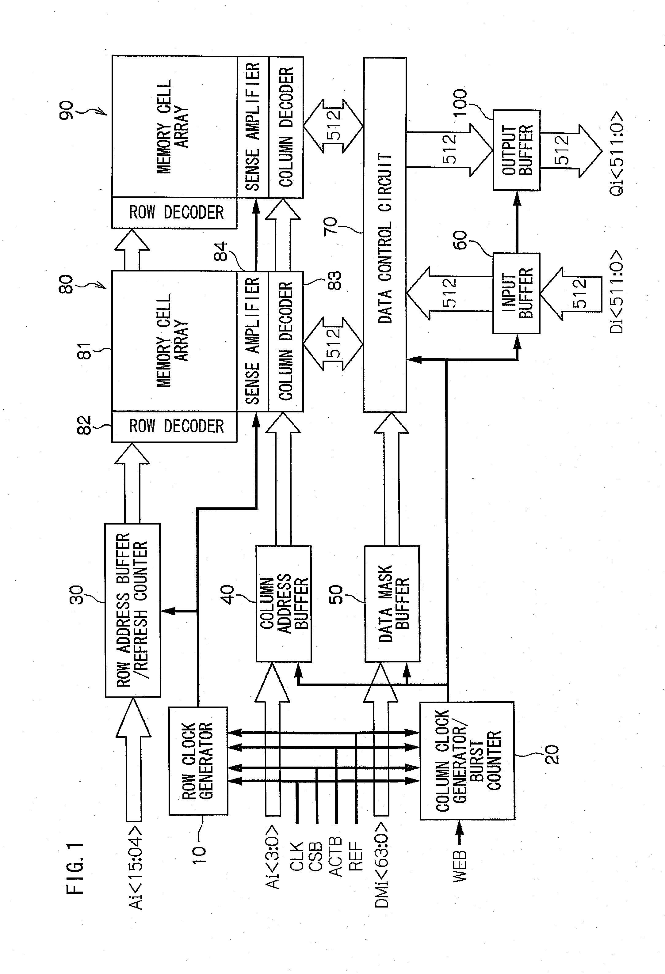
[0024]FIG. 1 is a view showing the configuration of the semiconductor memory device in which the present invention is implemented. The semiconductor memory device comprises the row clock generator 10 which generates the row clock, the column clock generator / burst counter 20 which generates the column clock or counts the burst, the row address buffer / refresh counter 30 which temporarily stores the 12-bit row address Ai or counts the number of refreshes, the column address buffer 40 which temporarily stores the 4-bit column address Ai, and the data mask buffer 50 which temporarily stores the data mask.

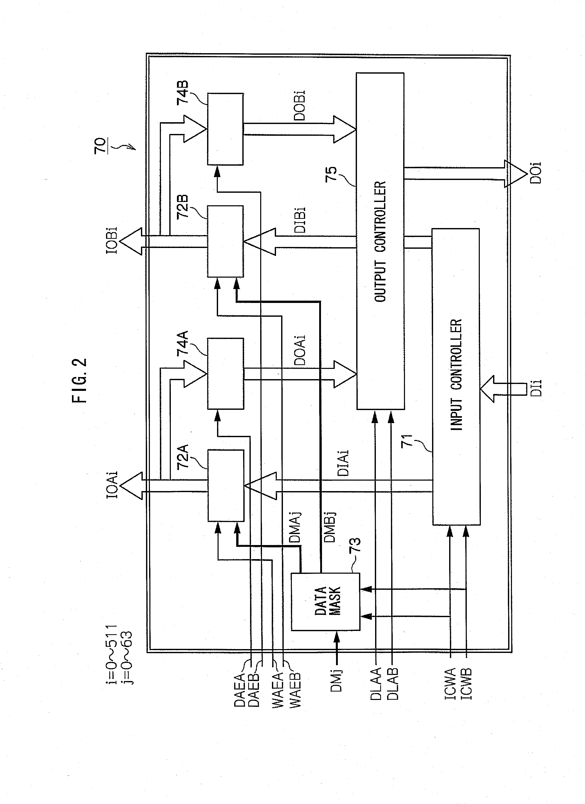
[0025]Also, the above-mentioned semiconductor memory device comprises the input buffer 60 which temporarily stores the data which is input from outside in a set of 512-bit signals, data control circuit 70 which outputs the data supplied by the input buffer 60, dividing it into two parallel data of a set of 512-bit signals each, or converting such two parallel data of a set of 512-bit sig...

second embodiment

[0060]Next is an explanation of the second embodiment of the present invention. Where there are common portions with the first embodiment, it is explained as such and details are omitted. In the first embodiment, the memory device has two memory banks. In the second embodiment, the memory device has four memory banks.

[0061]FIG. 5 is a view showing the configuration of the semiconductor memory device in which the present invention is implemented as the “second embodiment”. This semiconductor memory device has the third memory bank 180 and the fourth memory bank 190 in addition to the configuration shown in FIG. 1, and in stead of the data control circuit 70 shown in FIG. 1, it has the data control circuit 170. The third and the fourth memory banks 180 and 190 are configured in the same way as shown in FIG. 3.

[0062]FIG. 6 is a block diagram showing the configuration of the data control circuit 170. The data control circuit 170 comprises the input controller 171 which converts serial d...


PUM


Abstract

The semiconductor memory device proposed in the present invention comprises memory cells disposed in the row direction and the column direction, a plurality of first lines by which supply voltages are supplied in order to select memory cells disposed in the row direction among the plurality of cells, a plurality of second lines by which supply voltages are supplied in order to select memory cells disposed in the column direction among the plurality of cells, the data lines which input and output the data to the selected memory cells, the first power voltage supply circuit which supplies the predetermined supply voltages to the first lines corresponding with the externally input row address synchronizing with an act command, and the second power voltage supply circuit which supplies the predetermined supply voltages to the second lines corresponding with the externally input column address synchronizing with an act command. It also comprises m pieces of memory banks (m is a natural number larger than 2) which write or read the data into or from the memory cells which are selected one after another in the row or column directions, data input circuits in which multiple bits of serial data which is larger than 512 bits to be written in the m pieces of memory banks, data output circuits which reads the data from the m pieces of memory banks and output in a form of multiple bits of serial data which is larger than 512 bits, and data conversion circuits which convert the serial data input in the data input circuits to parallel data so that it can be written in each memory bank or to convert each parallel data read from each memory bank to serial data so that such data are supplied to the data output circuits.

Description

TECHNICAL FILED[0001]This invention is with respect to a semiconductor memory device, particularly a memory device which contains DRAM chips.BACKGROUND ART[0002]Conventionally, Dynamic Random Access Memories (DRAMs) are commonly used as semiconductor memory devices temporarily storing data. Compared to Static Random Access Memories (SRAMs), DRAMs have simpler circuits, can be easily integrated, and are lower in price. Therefore, DRAMs are most commonly used as main memories in computers.[0003]However, in spite of above-mentioned strengths, the performance of random access by DRAMs is not good. In order to deal with such weakness, there are newly proposed memory products which consecutively read data with different column addresses in high speed and re-write the data. (e.g., see attached patent document 1)[0004]The memory (DRAM) described in the patent document 1 consists of a plurality of memory cells distributed at crossing points of data lines and word lines in a matrix form and i...

Claims


Application Information

Patent Timeline
IPC IPC(8): G11C5/02G11C5/14G11C8/00G11C7/00
CPCG11C11/4076G11C11/408G11C11/4094G11C11/4097
Inventor NAKAOKA, YUJIIWASHITA, SHIN-ICHI
Owner RAMBUS INC
Why Eureka
Try Eureka