Bandpass filter and process of fabricating the same

a filter and bandpass technology, applied in the field of bandpass filters, can solve the problems of not being suitable for incorporation into a miniaturized device, ring resonators occupying a relatively large space, and likely to pass undesired frequency or fail to attenuate undesired frequency, and achieve excellent out-of-band rejection, sharp and wide bandpass, and improved near-band rejection.

Inactive Publication Date: 2010-05-13
MATSUSHITA ELECTRIC WORKS LTD
View PDF3 Cites 8 Cited by
  • Summary
  • Abstract
  • Description
  • Claims
  • Application Information

AI Technical Summary

Benefits of technology

[0004]In view of the above problem, the present invention has been achieved to provide a bandpass filter which is compact and efficient for rejecting out-of-band frequencies. The bandpass filter in accordance with the present invention include a bulk acoustic wave (BAW) filter composed of a plurality of piezoelectric resonators to give a specific frequency bandpass, and a patterned planer filter configured to attenuate frequencies near and outside the bandpass. The resonators, each including includes a piezoelectric element disposed between a lower electrode and an upper electrode, are connected in a ladder configuration between a first signal transmission path and a ground to provide the bandpass. The planar filter includes a strip line structure composed of a ground conductor, a dielectric layer on the ground conductor, and a strip line formed on the dielectric layer to define a second signal transmission path. The strip line is added with at least one stub composed of a loading segment extending in a spaced relation from the strip line and a tap segment extending from said strip line and merging at an intermediate portion of the loading segment between the opposite lengthwise ends thereof. The BAW filter and the planar filter are formed on a common substrate with the first and second transmission paths connected to each other. The BAW filter thus combined with the patterned planar filter added with the stub can improve a deep near-band rejection inherent to the BAW filter, exhibiting an excellent out-of-band rejection over certain adjacent frequency ranges outside of the bandpass, and therefore give a sharp and wide bandpass. Further, the planar filter is realized by making the use of the substrate common to the BAW filter, and is adds only a small space requirement to a compact structure inherent to the BAW filter, thereby maintaining the combination bandpass filter sufficiently compact. Especially, the addition of the stub to the strip line can shorten the length of the planar filter as well as improve an effect of attenuating the out-of-band frequencies.

Problems solved by technology

However, since each ring resonator is inherently given a relatively narrow rejection band, the combination of the ring resonators is likely to pass undesired frequency or fail to attenuate the undesired frequency to a practically admissible level.
Further, since each of the ring resonators is required to have a diameter of up to 1 cm for use in the UWB application, the combination of the ring resonator occupies a relatively large space and is therefore not suitable for incorporation into a miniaturized device.

Method used


Image

  • Bandpass filter and process of fabricating the same
  • Bandpass filter and process of fabricating the same
  • Bandpass filter and process of fabricating the same

Examples


Embodiment Construction

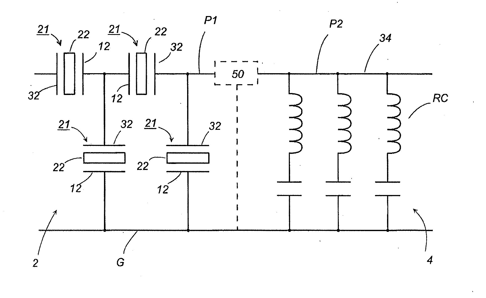
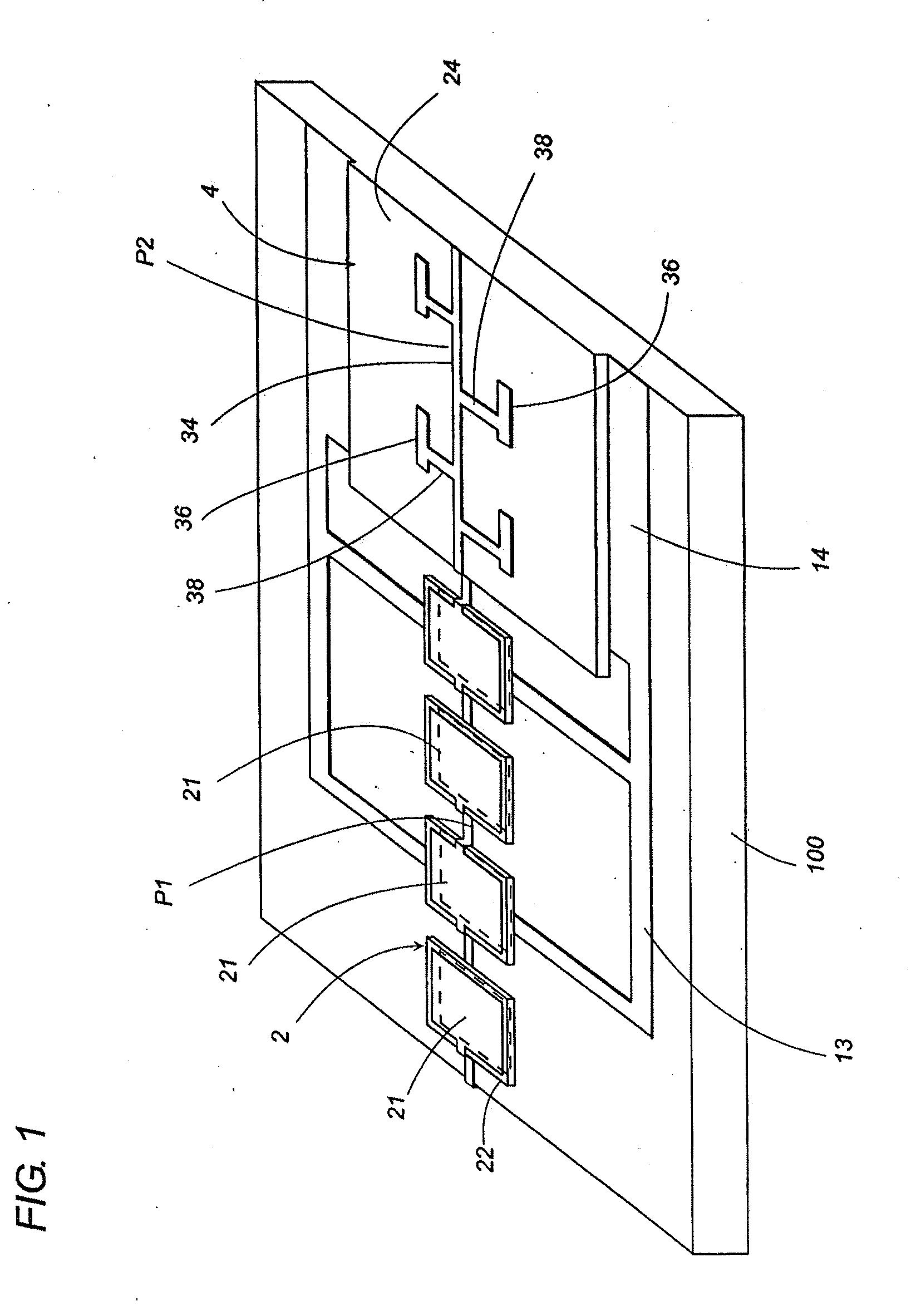
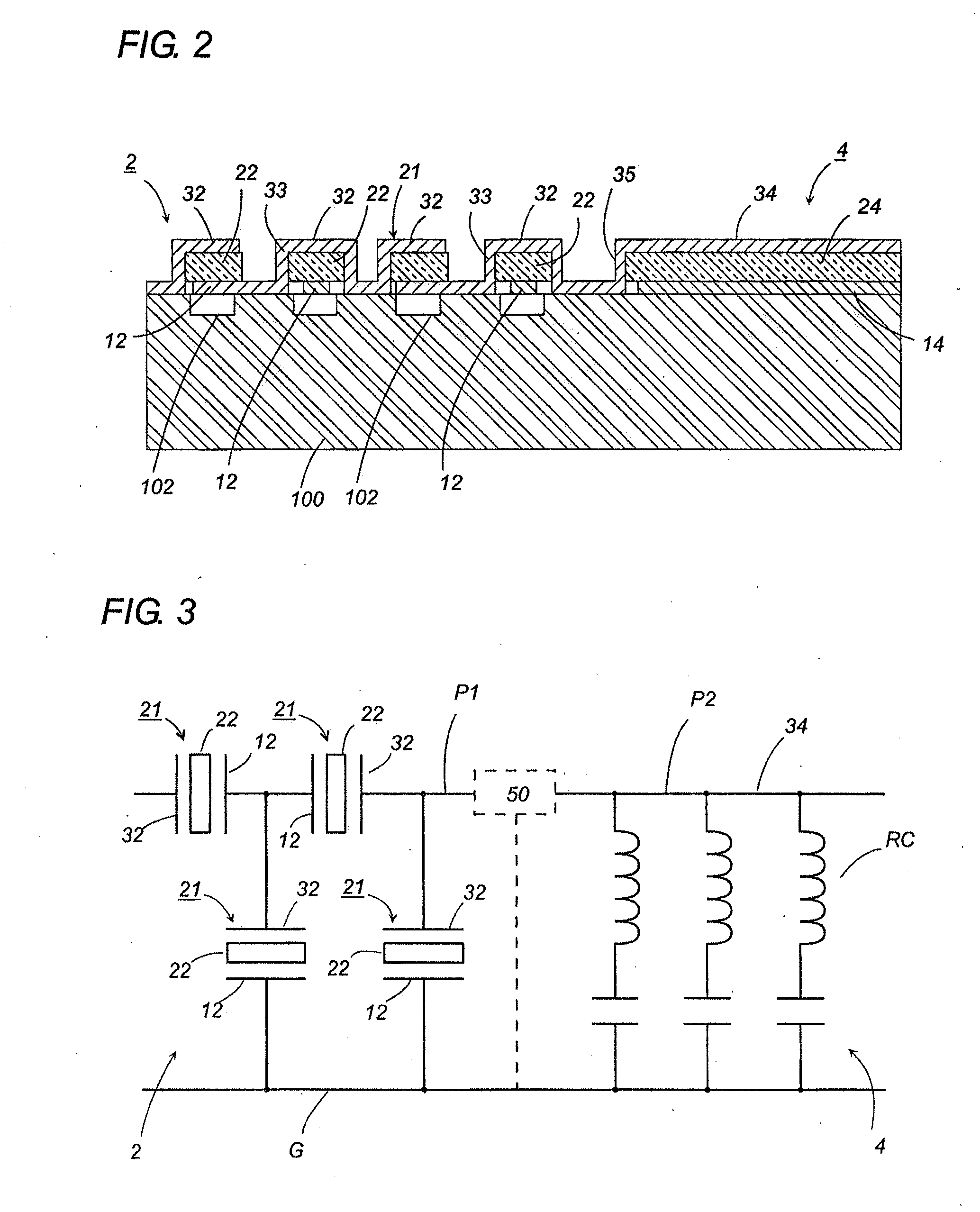
[0026]Referring now to FIGS. 1 and 2, there is shown a bandpass filter in accordance with a first embodiment of the present invention. The bandpass filter is designed for use in the ultra-wide band (UWB) application to have a bandpass in a frequency range of 3.5 GHz to 3.9 GHz, for example. The bandpass filter is a combination of a bulk acoustic wave (BAW) filter 2 and a planar patterned filter 4 which are formed on a common substrate 100 which is made of a semiconductor material of silicon, for example.

[0027]The BAW filter 2 includes a plurality of film bulk acoustic piezoelectric resonators 21 each composed of a piezoelectric element 22 disposed between a lower electrode 12 and an upper electrode 32. The resonators 21 are connected in a ladder configuration, as shown in FIG. 3, between a first signal transmission path P1 and a ground to provide the bandpass of the frequency. The substrate 100 is formed in its top surface with a plurality of cavities 102 disposed in closely adjacen...


PUM

PropertyMeasurementUnit
relative dielectric constantaaaaaaaaaa
frequencyaaaaaaaaaa
frequencyaaaaaaaaaa

Abstract

A bandpass filter includes a combination of a BAW filter and a patterned planar filter with stubs. The BAW filter is composed of a plurality of piezoelectric resonators to give a specific frequency bandpass, while the planer filter is configured to attenuate frequencies near and outside the bandpass. The resonators are connected in a ladder configuration between a first signal transmission path and a ground. The planar filter includes a strip line formed on a dielectric layer to define a second signal transmission path. The BAW filter and the planar filter are formed on a common substrate with the first and second transmission paths connected to each other. The BAW filter, in combination with the patterned planar filter added with the stub, can improve a deep near-band rejection inherent to the BAW filter, exhibiting an excellent out-of-band rejection over certain adjacent frequency ranges outside of the bandpass, and therefore give a sharp and wide bandpass.

Description

TECHNICAL FIELD[0001]The present invention is directed to a bandpass filter, particularly for use in an ultra-wide band (UWB) application with an excellent out-of-band rejection, and a process of fabricating the bandpass filter.BACKGROUND ART[0002]Recently, there has been an increased demand of developing the UWB technique to realize a high speed data transmission at several hundreds of mega bits per second within a permitted frequency range of 3.1 GHz to 10.6 GHz. In order to comply with regulations with regard to the UWB communication, a bandpass range is restricted to be 500 MHz or 25% of a central frequency, and is different from a specific bandpass around 1.6 GHz given to the GPS (global positioning system). Therefore, the UWB application necessitates a bandpass filter with good near-band rejection.[0003]Japanese Patent Publication (JP 2005-295316 A) proposes a bandpass filter available for the UWB application. The proposed bandpass filter includes a multiplicity of ring resona...

Claims


Application Information

Patent Timeline
Patent Type & Authority Applications(United States)
IPC IPC(8): H03H9/205H01P1/203H01L41/22H01L41/09H01L41/18H01L41/187H01L41/319H03H3/02H03H7/075H03H9/17H03H9/54
CPCH01P1/203H03H3/02H03H9/0542Y10T29/42H03H9/564H03H9/568H03H9/542
Inventor SUWA, ATSUSHISASABE, KOJINISHIMURA, FUTOSHIHAYASAKI, YOSHIKIMATSUSHIMA, TOMOAKIXIONG, SIBEIYOSHIHARA, TAKAAKIYAMAUCHI, NORIHIROSHIRAI, TAKEO
Owner MATSUSHITA ELECTRIC WORKS LTD
Why Eureka
Try Eureka