Power factor correction circuit

a power factor and correction circuit technology, applied in power conversion systems, climate sustainability, energy industry, etc., can solve problems such as noise, deterioration of efficiency, and increase heat generation, and achieve the effects of simplifying structure, simplifying noise generation, and improving efficiency

Inactive Publication Date: 2010-05-13
SANKEN ELECTRIC CO LTD
View PDF6 Cites 25 Cited by
  • Summary
  • Abstract
  • Description
  • Claims
  • Application Information

AI Technical Summary

Benefits of technology

[0017]The present invention is able to provide a power factor correction circuit that is capable of diffusing generated noise, improving efficiency, and simplifying structure.

Problems solved by technology

Although the recovery current is a short pulse current, it is large, and therefore, produces noise.
However, it converts energy that causes the noise into heat by the snubber circuit, and therefore, increases heat generation and deteriorates efficiency.

Method used


Image

  • Power factor correction circuit
  • Power factor correction circuit
  • Power factor correction circuit

Examples


embodiment 1

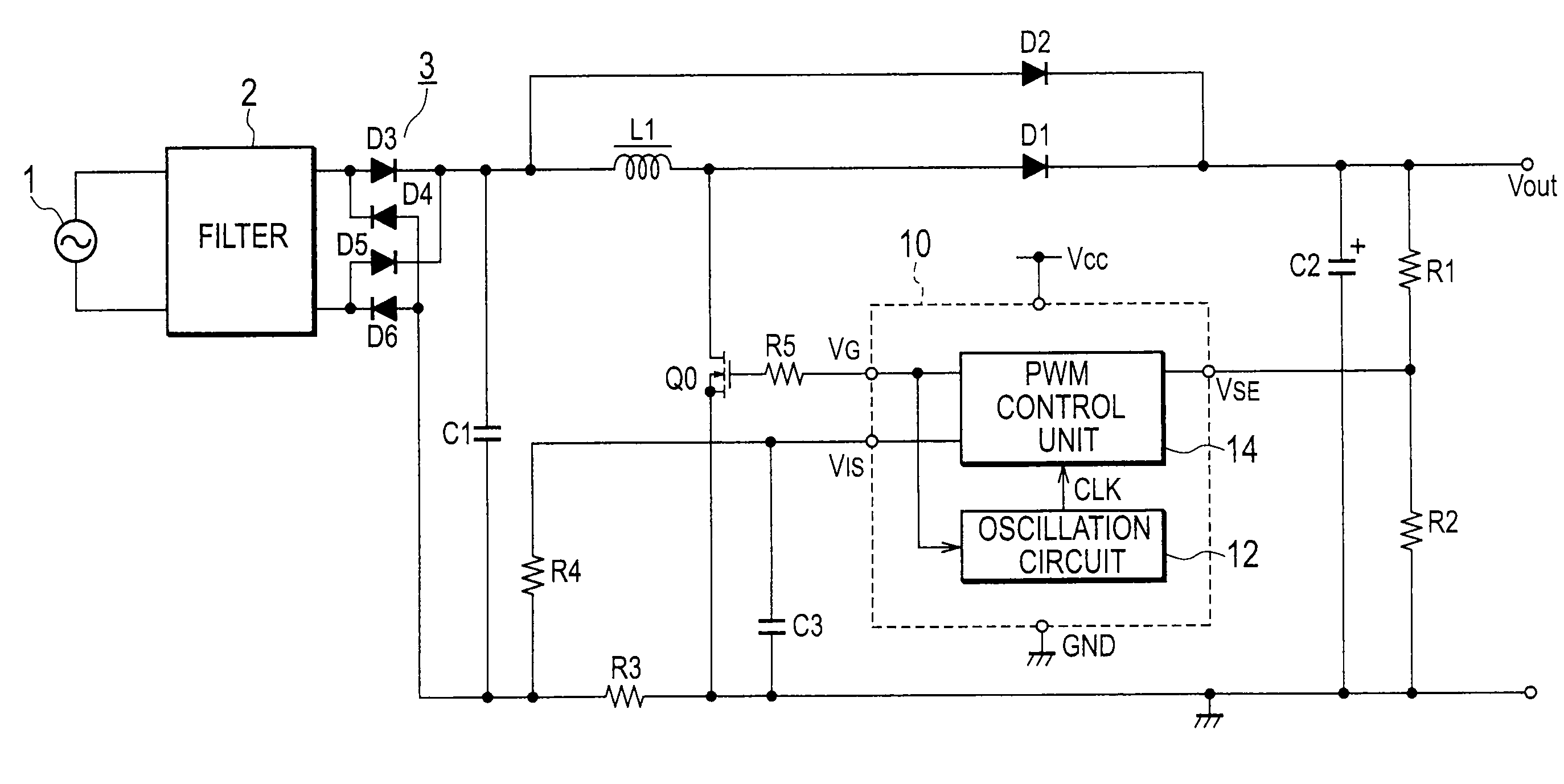
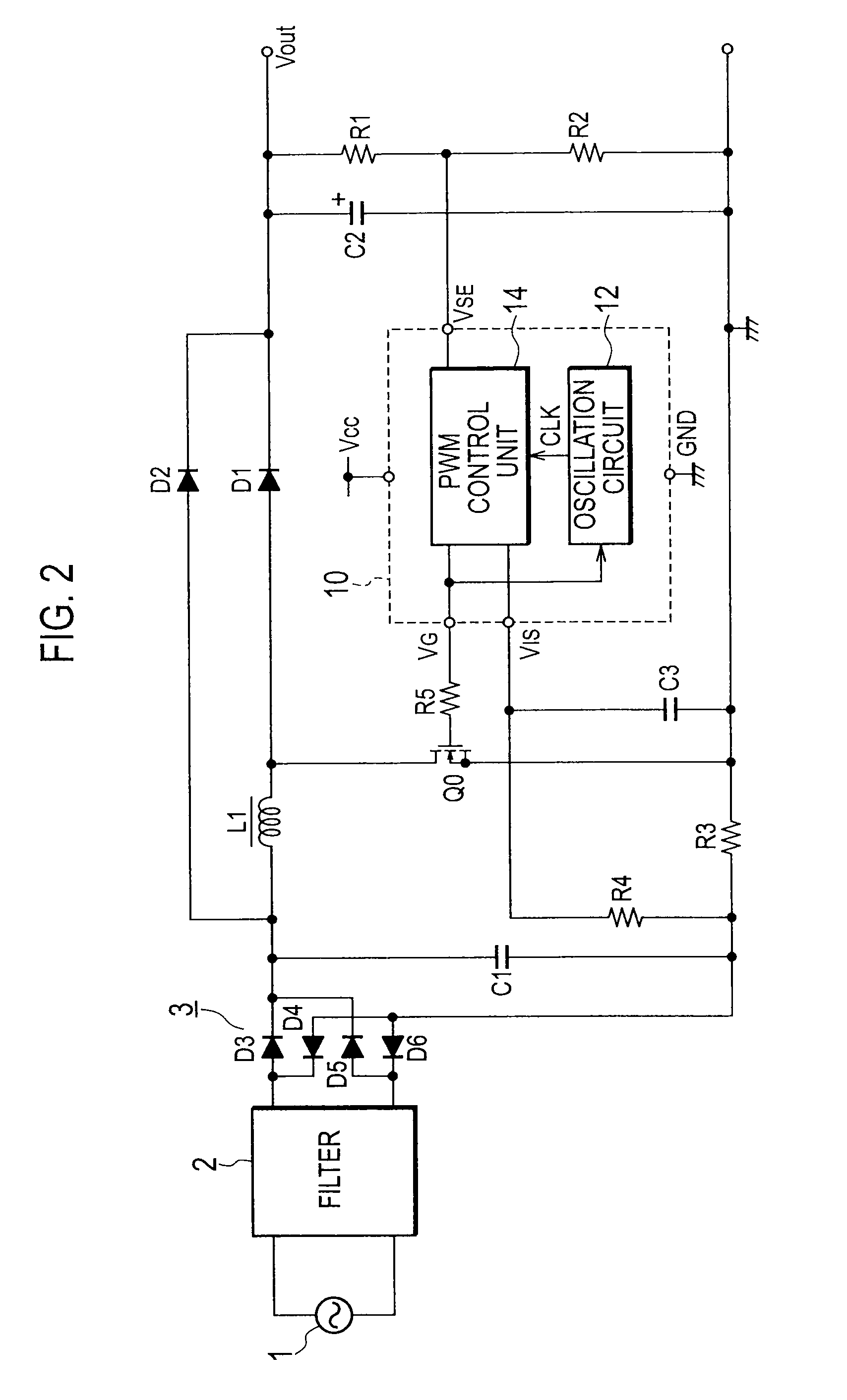
[0028]FIG. 2 is a view illustrating the power factor correction circuit according to Embodiment 1 of the present invention. The power factor correction circuit of Embodiment 1 illustrated in FIG. 2 is characterized in that, compared with the power factor correction circuit of the related art illustrated in FIG. 1, the resistors R6 and R7 connected to the output of the full-wave rectifier 3 are omitted and an output terminal VG of a PWM control unit 14 and an oscillation circuit 12 are connected to each other.

[0029]The oscillation circuit 12 generates a clock signal having a predetermined oscillation frequency, receives a PWM signal for a switching element Q0 from the output terminal VG of the PWM control unit 14, and according to the PWM signal, changes the predetermined oscillation frequency of the clock signal.

[0030]The PWM control unit 14 generates, at a period of the clock signal generated by the oscillation circuit 12 and according to a voltage value of a smoothing capacitor C2...

embodiment 2

[0050]FIG. 5 is a view illustrating an oscillation circuit arranged in a power factor correction circuit according to Embodiment 2 of the present invention. The oscillation circuit 12a of Embodiment 2 is characterized in that a series circuit having an FET Q8 and a constant current source IADJ is connected in parallel with an FET Q1. The remaining configuration of the oscillation circuit 12a illustrated in FIG. 5 is the same as that of the oscillation circuit of Embodiment 1 illustrated in FIG. 3, and therefore, the same parts are represented with the same reference marks to omit the explanations thereof.

[0051]Like Embodiment 1, an FET Q3 provides a current equal to a current passing through the FET Q1, and this current charges an oscillation capacitor Cosc. When an FET Q4 is OFF, an FET Q6 provides a current that is larger than the current passing through the FET Q3 by a predetermined magnification ratio, to discharge the oscillation capacitor Cosc.

[0052]When the FET Q8 turns off, ...

embodiment 3

[0056]FIG. 7 is a view illustrating an oscillation circuit arranged in a power factor correction circuit according to Embodiment 3 of the present invention. The oscillation circuit 12b illustrated in FIG. 7 is characterized in that there are arranged an operational amplifier AM1, an FET Q10, and resistors R10 and R11 instead of the constant current sources Iosc and IADJ of the oscillation circuit 12 as illustrated in FIG. 3.

[0057]The drain of an FET Q1 is connected to the drain of the FET Q10, and the source of the FET Q10 is connected to an end of the resistor R10 and an inverting terminal (depicted by “−”) of the operational amplifier AM1. The other end of the resistor R10 is connected to an end of the resistor R11 and the drain of an FET Q8. The other ends of the resistor R11 and FET Q8 are grounded. A non-inverting terminal (depicted by “+”) of the operational amplifier AM1 is connected to a reference power source Vr and an output terminal of the operational amplifier AM1 is con...


PUM


Abstract

A power factor correction circuit includes a rectifier 3 to rectify an AC voltage of an AC power source 1, a first series circuit connected in parallel with an output of the rectifier and having a step-up reactor L1 and a switching element Q0 that are connected in series, a second series circuit connected in parallel with the switching element and having a rectifying diode D1 and a smoothing capacitor C2 that are connected in series, an oscillation circuit 12 to generate a clock signal CLK having a predetermined oscillation frequency, and a control circuit 10 to generate, at the period of the clock signal generated by the oscillation circuit and according to a voltage value of the smoothing capacitor, a drive signal for driving the switching element. The oscillation circuit changes the predetermined frequency according to the drive signal for the switching element.

Description

TECHNICAL FIELD[0001]The present invention relates to a step-up-type power factor correction circuit having a power factor correction function.BACKGROUND TECHNOLOGY[0002]Converting an AC voltage of an AC power source into a DC voltage through a rectifier and smoothing capacitor results in distorting an input current and deteriorating a power factor. For this, a step-up chopper circuit consisting of a step-up reactor, a switching element, a rectifying diode, and a smoothing capacitor is connected to an output of the rectifier, to form a power factor correction circuit to reduce the distortion of an input current.[0003]A control method for the power factor correction circuit may be a DCM (Discontinuous Conduction Mode) method that turns on the switching element for a predetermined period to pass a current through the step-up reactor, detects that the current passing through the step-up reactor is zeroed after the switching element turns off, and again turns on the switching element, o...

Claims


Application Information

Patent Timeline
Patent Type & Authority Applications(United States)
IPC IPC(8): H02M7/06
CPCY02B70/126H02M1/4225Y02B70/10Y02P80/10
Inventor OSAKA, SHOHEI
Owner SANKEN ELECTRIC CO LTD
Why Eureka
Try Eureka