

Optical element molding die and method for molding optical element
a technology of optical elements and molding dies, which is applied in the manufacture of butter, glass pressing apparatus, lenses, etc., can solve the problems of difficult to completely remove dust, inability to obtain desired microshape, and inability to reduce dust, etc., and achieves high accuracy and exceptional durability.
- Summary
- Abstract
- Description
- Claims
- Application Information
AI Technical Summary
Benefits of technology
Problems solved by technology
Method used
Image

Examples
first embodiment
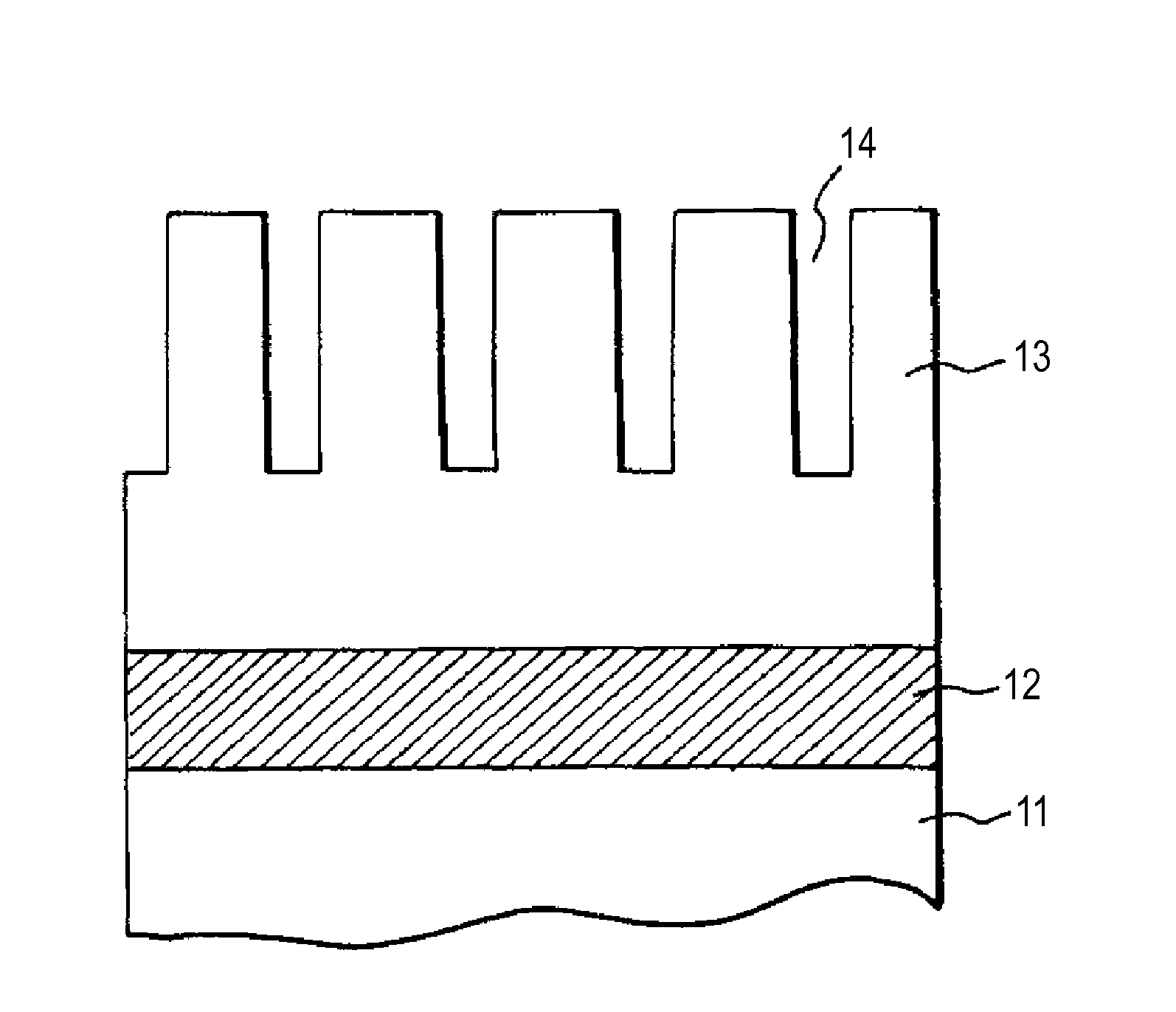
[0020]The first embodiment of the mold for optical element molding in accordance with the invention will be described with reference to FIG. 1.
[0021]FIG. 1 illustrates schematically a cross section of the first embodiment of the optical element molding die in accordance with aspects of the invention.
[0022]In FIG. 1, the reference numeral 11 stands for a substrate having a t least a surface composed of a material with a negative standard electrode potential, 12—a protective layer formed on the substrate 11, and 13—an anodic oxidation layer provided on the protective layer 12. A large number of holes 14 are formed by conducting anodic oxidation in the anodic oxidation layer 13. The holes are opened in the direction perpendicular to the surface of the anodic oxidation layer. In FIG. 1, the substrate 11 has a flat shape, but such a shape is not limiting, and the substrate may also have a curved shape. The shape of the entire optical element molding die is not particularly limited and ma...
second embodiment
[0042]The second embodiment of the optical element molding die in accordance with aspects of the invention will be described below.
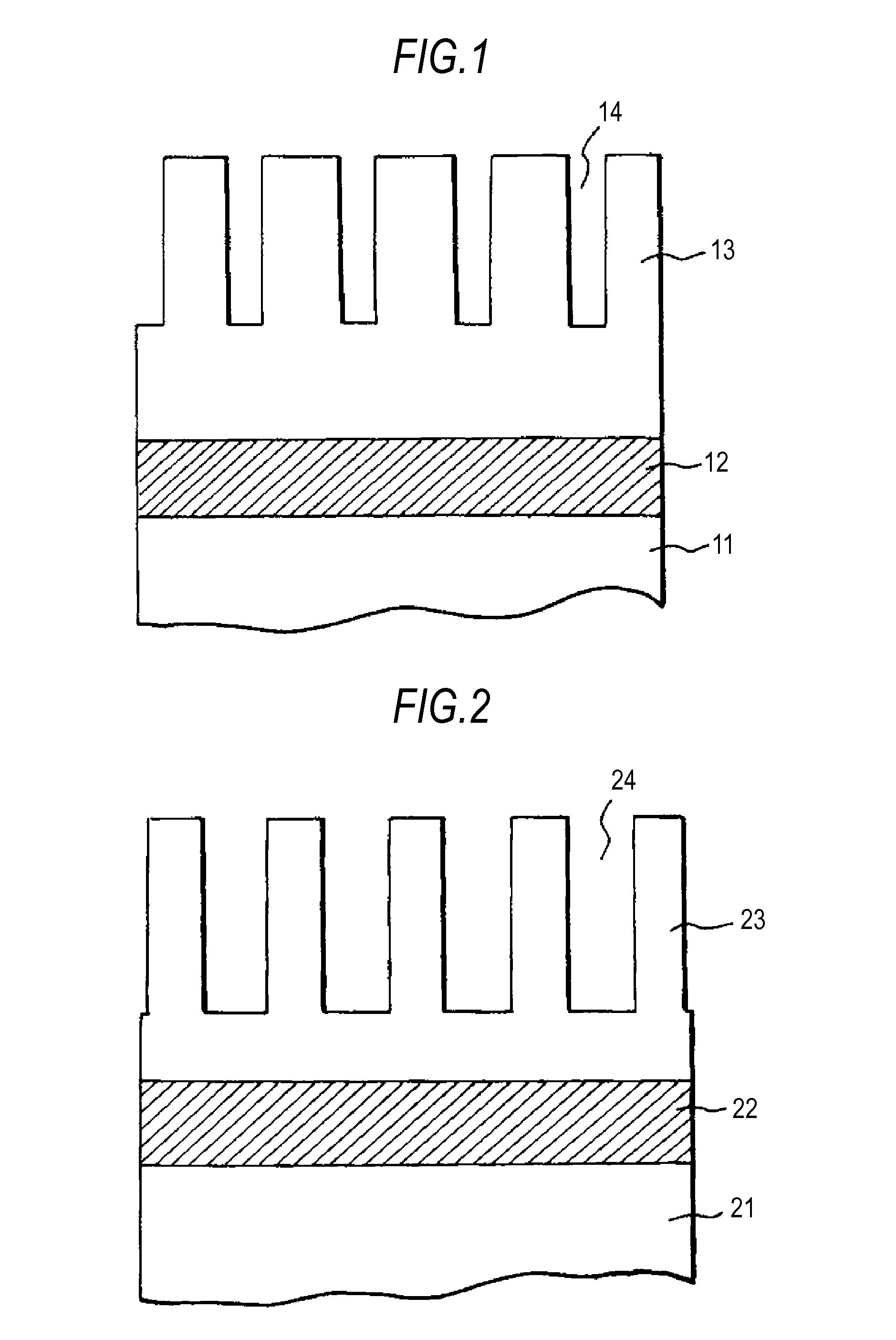
[0043]In the present embodiment, the diameter of a plurality of holes formed during anodic oxidation of aluminum is enlarged by etching in the anodic oxidation layer. The optical element molding die that has the above-described structure will be explained with reference to FIG. 2. The first embodiment and second embodiment have many common features, the explanation of these features will be omitted, and only features that are different from those of the first embodiment will be explained.
[0044]FIG. 2 is an enlarged schematic drawing illustrating the cross-section of a plurality of protrusions at a substrate having the concave-convex structure of the present embodiment. In the present embodiment, similarly to the first embodiment, an anodic oxidation layer 23 is formed on a protective layer 22 that has been provided on a substrate 21. The diameter of a ve...
third embodiment
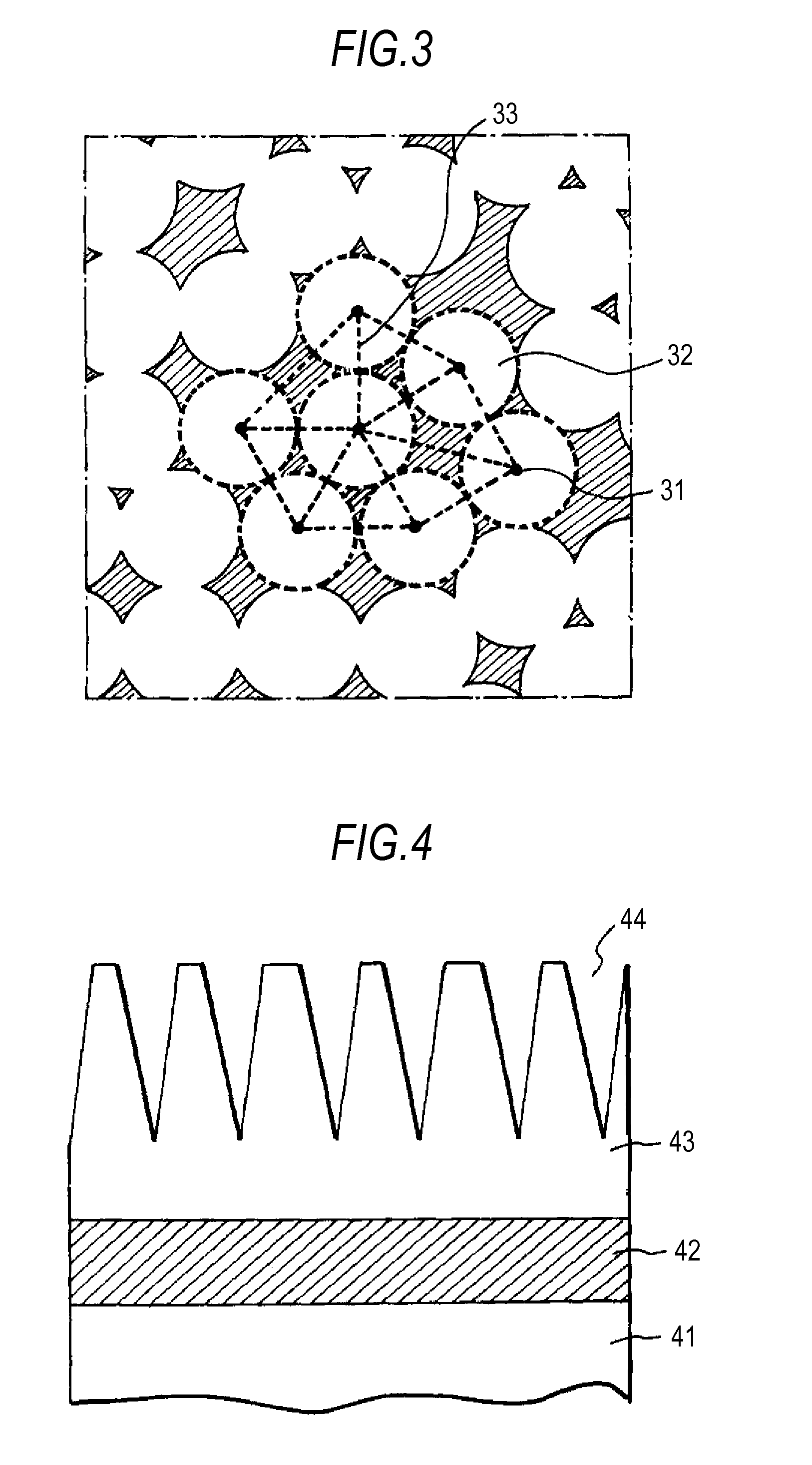
[0048]In the present embodiment, an optical element will be explained that is molded by a molding process using an optical element molding die fabricated by a method similar to that of the second embodiment, this optical element having a plurality of concave-convex structures obtained by transferring the surface of the optical element molding die. By using the optical element molding die that is produced by a method possible to inhibit the occurrence of pinholes. Therefore, the concave-convex structure can be produced according to the designed values at the die, thereby making it possible to obtain an optical element according to the designed values.
[0049]Generally, when two substances with different refractive indexes and a pitch shorter than a wavelength are mixed, the refractive index n12 in the mixing region can be represented with Equation (2) below by the refractive indexes (n1, n2) of the two substances and volume (ff1, ff2) occupied by each substance per unit volume.
n12=ff1×...
PUM
| Property | Measurement | Unit |
|---|---|---|
| temperature | aaaaa | aaaaa |
| voltage | aaaaa | aaaaa |
| negative standard electrode potential | aaaaa | aaaaa |
Abstract
Description
Claims
Application Information