Method and apparatus for wafer bonding with enhanced wafer mating

a technology of enhanced wafers and wafers, applied in the direction of manufacturing tools, controlling lamination, transportation and packaging, etc., can solve the problems of over-all processing yield and manufacturing cost of the so produced, the final product where the wafer alignment may be degraded to more than several micron accuracy levels, and the influence of the cost of electronic products incorporating these devices

Active Publication Date: 2010-05-20
SUSS MICRO TEC LITHOGRAPHY
View PDF5 Cites 61 Cited by
  • Summary
  • Abstract
  • Description
  • Claims
  • Application Information

AI Technical Summary

Benefits of technology

[0009]In general, in another aspect, the invention features a method for bonding semiconductor structures including the following. First, positioning a first surface of a first semiconductor structures directly opposite to and at a first distance from a first surface of a second semiconductor structure. Next, aligning the first surfaces of the first and second semiconductor structures parallel to each other to submicron alignment accuracy. Next, applying pressure to a second surface of the first semiconductor structure via a pressurized gas flowing through a port terminating at the second surface and bowing the first surface of the first semiconductor structure toward the first surface of the second semiconductor structure. The second surface of the first semiconductor structure is opposite to the first surface. Next, measuring the force applied to the second surface of the first semiconductor structure and then moving the first surface of the second semiconductor structure toward the first surface of the first semiconductor structure until the measured force reaches a set value. Next, controlling the velocity of the second semiconductor motion so that when the first surfaces are brought in atomic contact and a bond interface is formed, the bond interface propagates radially across the first surfaces at a set rate. Next, reducing the pressure of the pressurized gas when the first surfaces of the first and second semiconductor structures are in full contact with each other and then clamping the first and second semiconductor structures together within a fixture tool and then bonding the clamped first and second semiconductor structures.

Problems solved by technology

The overall processing yield and manufacturing cost of the so produced semiconductor devices and ultimately the cost of the electronic products that incorporate these devices depend greatly upon the quality of the wafer-to-wafer bond.
However, the follow-up steps of the bonding process distort the submicron accuracy of the initial alignment resulting in a final product where the wafer alignment may be degraded to more than several micron accuracy level.

Method used


Image

  • Method and apparatus for wafer bonding with enhanced wafer mating
  • Method and apparatus for wafer bonding with enhanced wafer mating
  • Method and apparatus for wafer bonding with enhanced wafer mating

Examples


Embodiment Construction

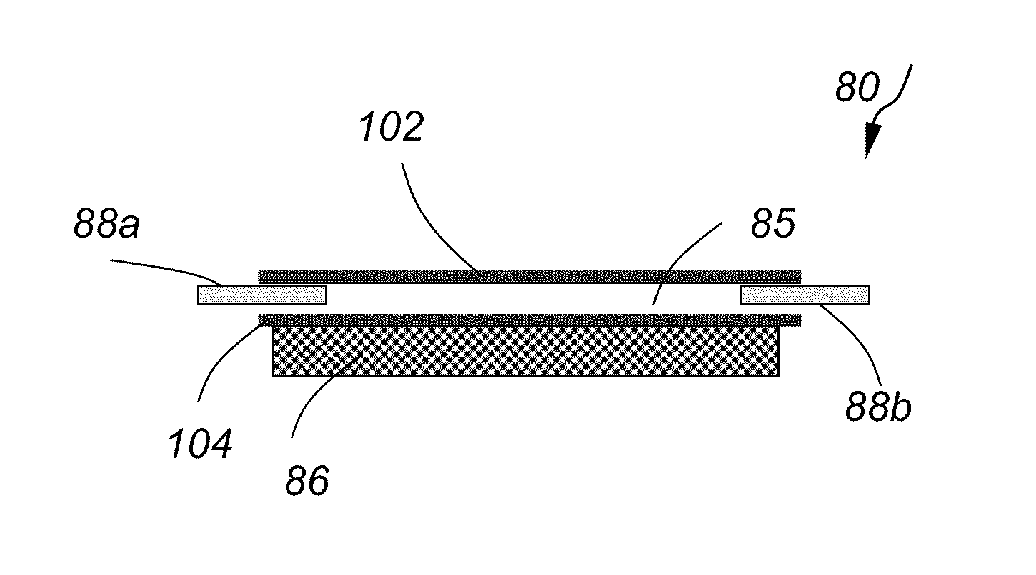
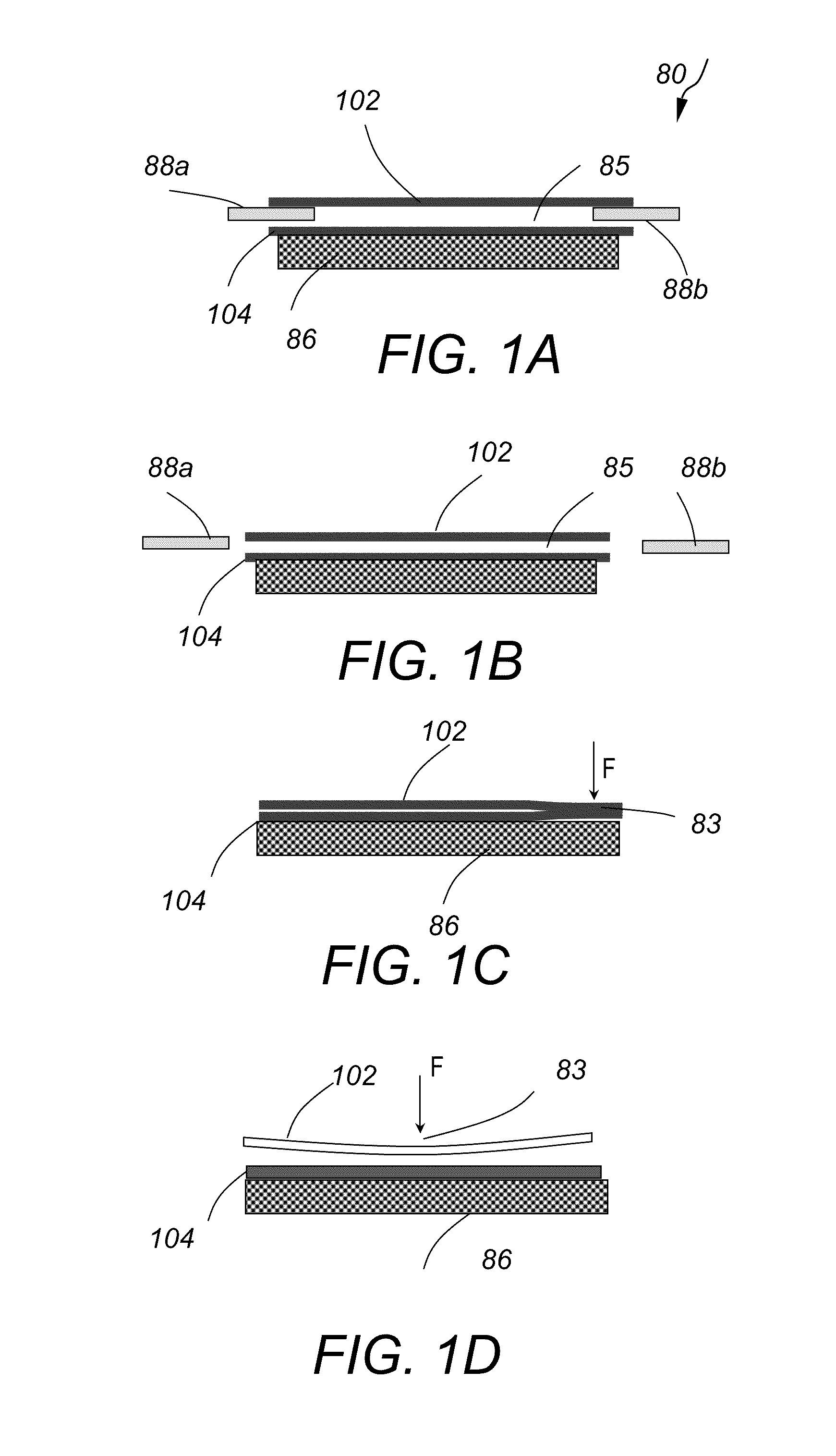
[0035]Referring to FIG. 1A, in a typical direct wafer bonding process 80, wafers 102, 104 are oriented horizontally and are aligned parallel to each other. The lower wafer104 is placed face up on a flat lower carrier (chuck) 86. The upper wafer 102 is placed face down on mechanical spacers 88a, 88b. The proximity gap 85 between the wafers is defined by the spacer thickness and position. Next, the spacers 88a, 88b are removed and the upper wafer 82 floats on top of the lower wafer 85 due to the air cushion 85 between the two flat surfaces, as shown in FIG. 1B. Next, a force F is applied at one single point 83 (typically at wafer edge, shown in FIG. 1C, or center, shown in FIG. 1D) to bring the wafers 102, 104 in close proximity or atomic contact and initiate the bonding based on Van-der-Waals forces. A linear or circular bond-front propagates, moving the air out of the contact interface and leaving the surfaces in atomic contact.

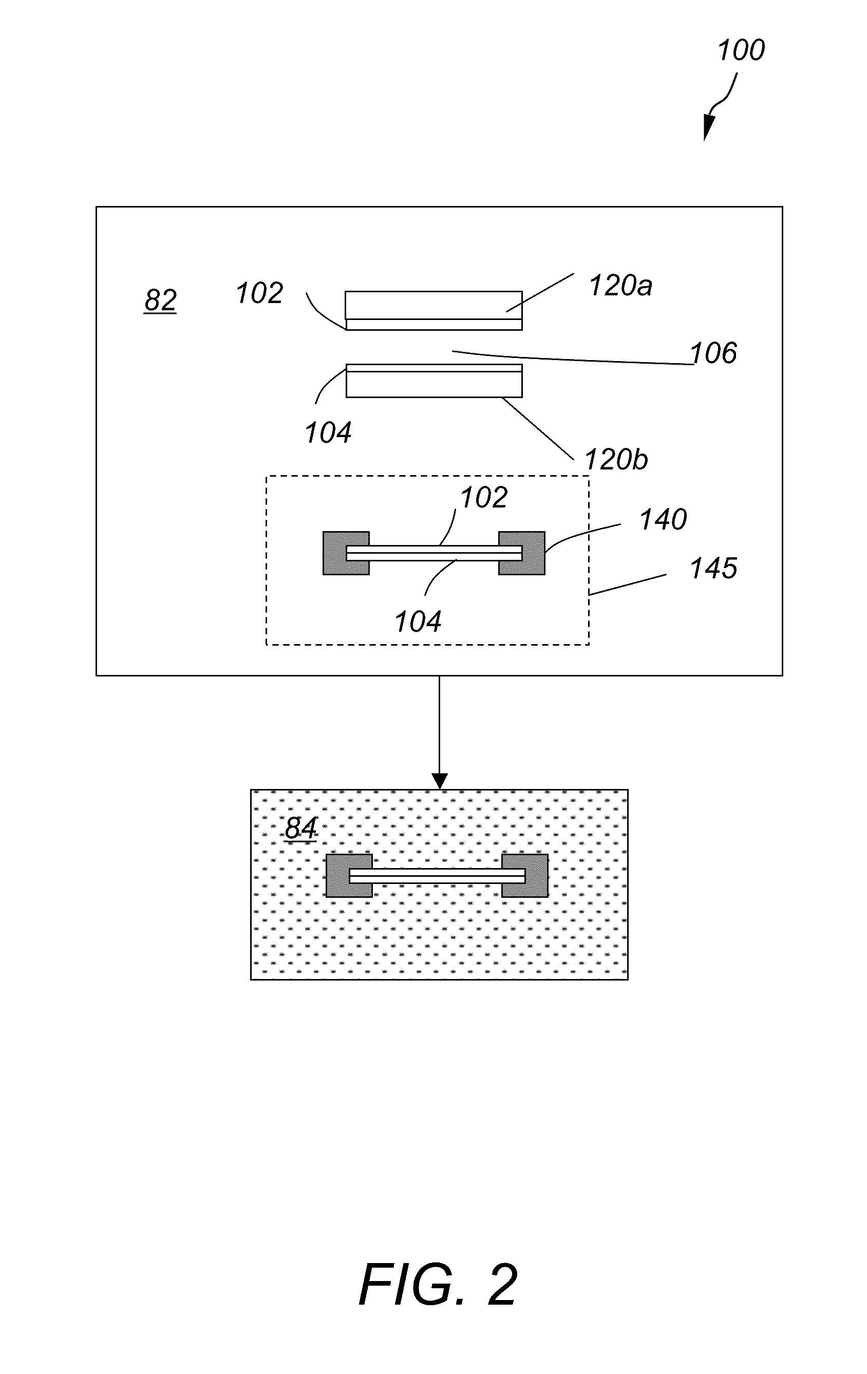
[0036]Referring to FIG. 2, an improved wafer bonding eq...


PUM

PropertyMeasurementUnit
distanceaaaaaaaaaa
distanceaaaaaaaaaa
pressureaaaaaaaaaa

Abstract

An improved wafer-to-wafer bonding method includes aligning an upper and a lower wafer and initiating a bond at a single point by applying pressure to a single point of the upper wafer via the flow of pressurized gas through a port terminating at the single point. The bond-front propagates radially across the aligned oppositely oriented wafer surfaces at a set radial velocity rate bringing the two wafer surfaces into full atomic contact by controlling the gas pressure and/or controlling the velocity of the motion of the lower wafer up toward the upper wafer.

Description

CROSS REFERENCE TO RELATED CO-PENDING APPLICATIONS[0001]This application claims the benefit of U.S. provisional application Ser. No. 61 / 115,101 filed Nov. 16, 2008 and entitled “METHOD AND APPARATUS FOR WAFER BONDING WITH ENHANCED WAFER MATING”, the contents of which are expressly incorporated herein by reference.FIELD OF THE INVENTION[0002]The present invention relates to an improved method and apparatus for semiconductor wafer bonding, and more particularly to industrial-scale semiconductor wafer bonding that provides enhanced wafer mating.BACKGROUND OF THE INVENTION[0003]Wafer-to-wafer (W2W) bonding is deployed in a wide range of semiconductor process applications for forming semiconductor devices. Examples of semiconductor process applications where wafer-to-wafer bonding is applied include substrate engineering and fabrication of integrated circuits, packaging and encapsulation of micro-electromechanical-systems (MEMS) and stacking of many processed layers (3D-integration) of p...

Claims


Application Information

Patent Timeline
Patent Type & Authority Applications(United States)
IPC IPC(8): B32B37/14
CPCH01L21/187Y10T29/49131H01L21/67092H01L21/30H01L23/12B81B7/00
Inventor GEORGE, GREGORY
Owner SUSS MICRO TEC LITHOGRAPHY
Why Eureka
Try Eureka