Substrate mounting table and substrate processing apparatus having same

a technology for processing apparatus and substrate, which is applied in the direction of electrical equipment, basic electric elements, electric discharge tubes, etc., can solve the problems of warping of the mounting table, insufficient contact of the mounted wafer, and difficulty in flattening the mounting table, so as to improve the in-plane temperature uniformity of the substrate and prevent deposits

Inactive Publication Date: 2010-05-20
TOKYO ELECTRON LTD
View PDF29 Cites 34 Cited by
  • Summary
  • Abstract
  • Description
  • Claims
  • Application Information

AI Technical Summary

Benefits of technology

[0011]Further, the present invention provides a substrate mounting table capable of improving an in-plane temperature uniformity of a su...

Problems solved by technology

Moreover, in the case of carrying out a waferless dry cleaning in a chamber of the plasma processing apparatus, it is required to increase the temperature of the mounting table rather than cooling it by the coolant.
However, according to the technique, a cavity as the heat transfer gas chamber is provided and, thus, it is difficult to machine the mounting table to be flat.
Moreover, the mounting table is warped by the pressure difference when the cavity is kept vacuum.
These may cause insufficient contact of the mounted wafer with the mounting table to deteriorate the...

Method used


Image

  • Substrate mounting table and substrate processing apparatus having same
  • Substrate mounting table and substrate processing apparatus having same
  • Substrate mounting table and substrate processing apparatus having same

Examples


first embodiment

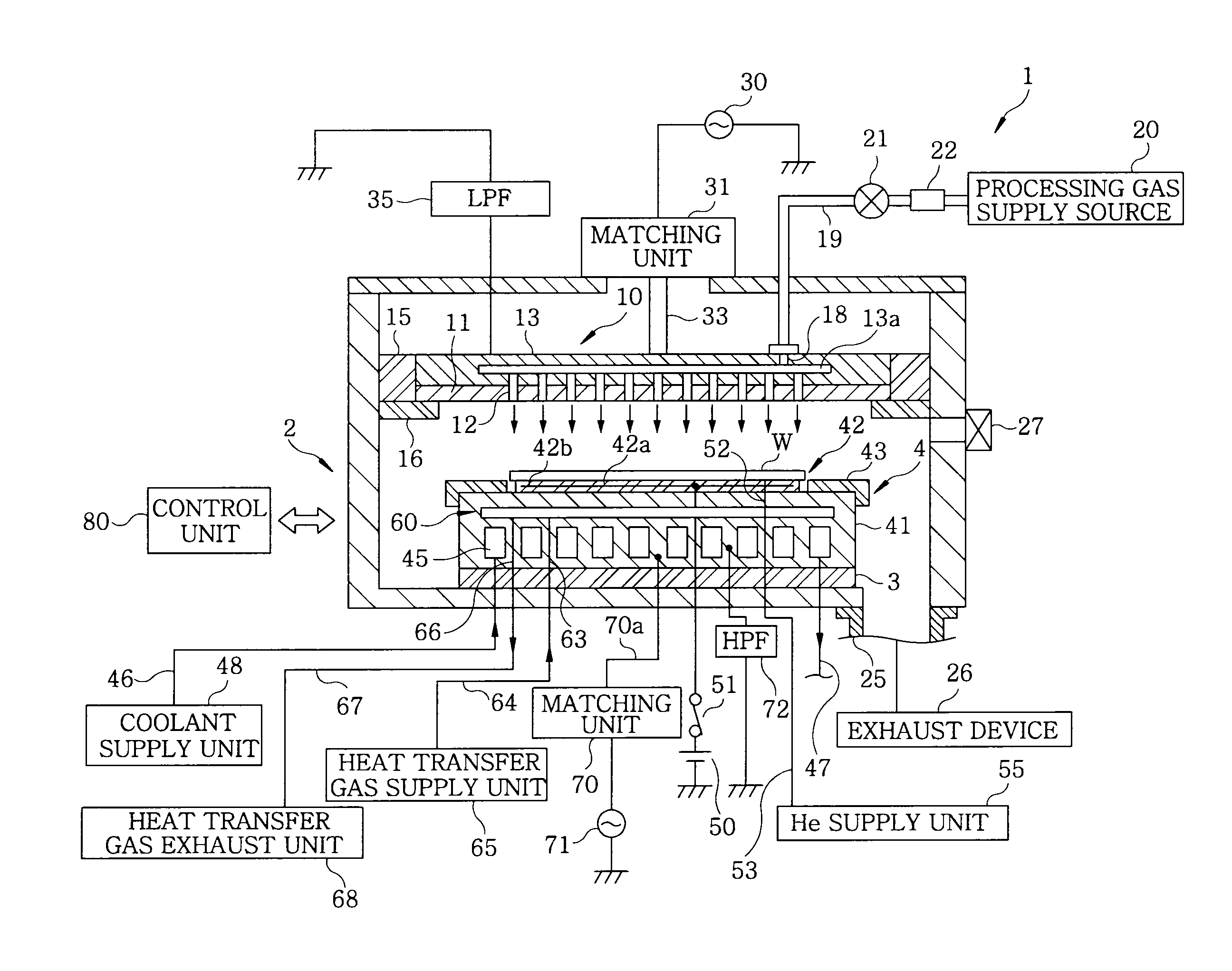
[0026]FIG. 1 is a cross sectional view showing a plasma processing apparatus 1 including a wafer mounting table (substrate mounting table) 4 in accordance with a first embodiment of the present invention.

[0027]The plasma processing apparatus 1 is a parallel plate type etching apparatus in which electrode plates are arranged in an upper and a lower portion to face each other in parallel and a capacitively coupled plasma is produced by a high frequency electric field generated between the electrodes.

[0028]The plasma processing apparatus 1 includes a cylindrical chamber 2, the surface of which is made of, e.g., an anodically oxidized aluminum. In a bottom portion of the plasma processing apparatus 1, the wafer mounting table (substrate mounting table) 4 in accordance with the first embodiment is provided via an insulating member 3 formed of, e.g., a ceramic or the like. A target substrate formed of, e.g., a semiconductor wafer W, is mounted on the wafer mounting table 4. The wafer moun...

second embodiment

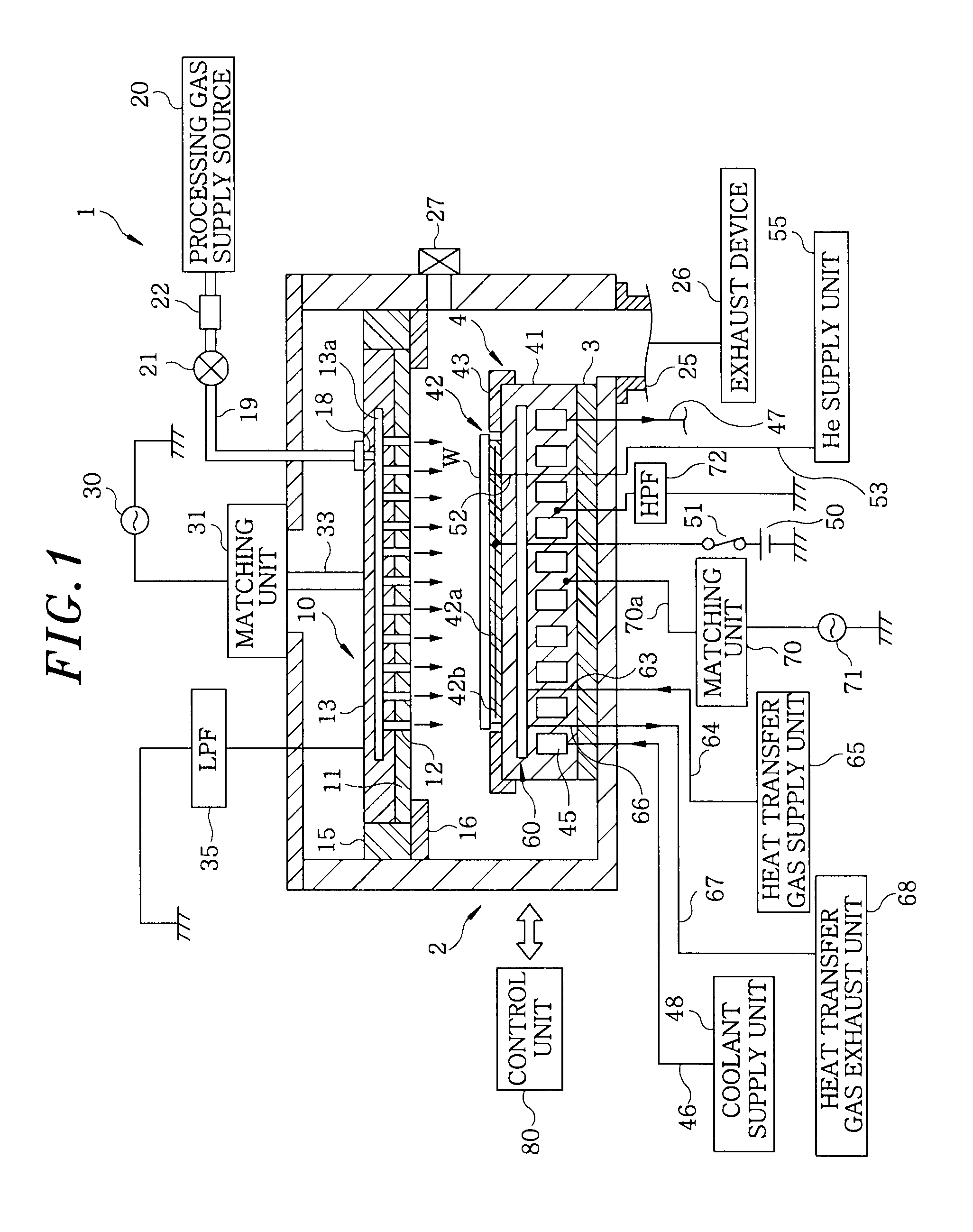
[0065]Next, a wafer mounting table (substrate mounting table) 4′ in accordance with a second embodiment of the present invention will be described. FIG. 6 is a cross sectional view showing the wafer mounting table 4′ in accordance with the second embodiment of the present invention. In the wafer mounting table 4′, a heat transfer control part 60′ is horizontally provided between the coolant circulation path 45 and the electrostatic chuck 42. The heat transfer control part 60′ includes a cavity portion 61′ provided therein to correspond to the wafer W, the cavity portion 61′ having a circular plate shape of a diameter greater than that of the wafer W. The cavity portion 61′ is concentrically divided into sub cavity portions, i.e., a central and an outer cavity portion 61a and 61b by a ring-shaped dividing member 61c. Solid members 62a and 62b are filled in the central and the outer cavity portion 61a and 61b, respectively. Like the solid member 62, each of the solid members 62a and 6...

third embodiment

[0076]Next, a wafer mounting table (substrate mounting table) 4″ in accordance with a third embodiment of the present invention will be described. FIG. 7 is a cross sectional view showing the wafer mounting table 4″ in accordance with the third embodiment of the present invention. In the wafer mounting table 4″, a heat transfer control part 60″ is horizontally provided between the coolant circulation path 45 and the electrostatic chuck 42. The heat transfer control part 60″ includes a cavity portion 61″ provided in the mounting table main body 41 to correspond to the wafer W, the cavity portion 61″ having a circular plate shape of a diameter greater than that of the wafer W. A solid member 62″ as a single unit is filled in the cavity portion 61″. Like the solid member 62, the solid members 62″ is made of, e.g., a porous ceramic and has a plurality of pores that communicate with one another.

[0077]The solid member 62″ may have a nonuniform porosity distribution in an in-plane directio...


PUM

PropertyMeasurementUnit
Heightaaaaaaaaaa
Pressureaaaaaaaaaa
Heataaaaaaaaaa

Abstract

A substrate mounting table includes a mounting table main body, a mounting unit provided at an upper portion of the mounting table main body, a heat source transferring a (cold) heat to the upper portion of the mounting table main body, and a heat transfer control part. The heat transfer control part includes a cavity portion provided in the mounting table main body to correspond to the mounted substrate, and a solid member filled in the cavity portion and having pores communicating with one another. The heat transfer control part controls a heat transfer level from the heat source by supplying or exhausting a heat transfer gas to or from the cavity portion. A controller controls the supplying and the exhausting of the heat transfer gas to and from the cavity portion by a heat transfer gas supply unit and a heat transfer gas exhaust unit, respectively.

Description

CROSS-REFERENCE TO RELATED APPLICATIONS[0001]This application claims priority to Japanese Patent Application No. 2008-297280 filed on Nov. 20, 2008, the entire contents of which are incorporated herein by reference.FIELD OF THE INVENTION[0002]The present invention relates to a substrate mounting table on which a substrate such as a semiconductor wafer or the like is mounted; and a substrate processing apparatus for performing a processing, e.g., a dry etching on a substrate mounted on the substrate mounting table.BACKGROUND OF THE INVENTION[0003]In the manufacturing process of a semiconductor device, a target substrate, e.g., a semiconductor wafer, is subjected to a plasma processing such as a dry etching, a sputtering, a chemical vapor deposit (CVD), or the like. For example, in a plasma etching process, a mounting table for mounting a wafer thereon is provided inside a chamber and the wafer is electrostatically attracted to and held by an electrostatic chuck which constitutes an u...

Claims


Application Information

Patent Timeline
IPC IPC(8): H01L21/306
CPCH01J37/32431H01L21/67109H01J2237/2001
Inventor MAKABE, TOSHIYUKIOKAJO, TAKETOSHI
Owner TOKYO ELECTRON LTD
Why Eureka
Try Eureka