MSD integrated circuits with trench contact structures for device shrinkage and performance improvement
- Summary
- Abstract
- Description
- Claims
- Application Information
AI Technical Summary
Benefits of technology
Problems solved by technology
Method used
Image


Examples
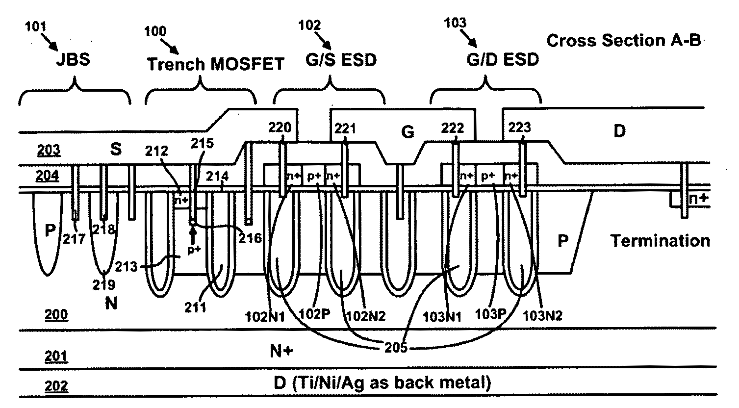
first embodiment
[0020]FIG. 2B is another cross-section C-D of the first embodiment as shown in FIG. 2C. The only difference between FIG. 2B and FIG. 2A is that there is an open area 250 of the drain metal on the top of the termination. A conventional metal field plate in the termination is provided to sustain breakdown voltage.
[0021]FIG. 2C is a top view of the first embodiment which shows Gate-Drain diode across termination with the open areas 250 in FIG. 2B of the drain metal. These open areas allow electrical field penetrate through the oxides during avalanche, and thus make benefits to avoid avalanche degradation caused by the metal field plate cross over the termination as shown in FIG. 2A.
[0022]FIG. 3 is a normalized measurement result of the relationship between breakdown voltage and metal width cross over metal field plate termination, which shows that breakdown voltage will be degraded when metal width W is greater than Sum, It means that electrical field underneath the cross-over metal ca...
second embodiment
[0023]FIG. 4A is the cross-section A-B of the present invention. The only difference between the structure of FIG. 4A and FIG. 2.A is that the embedded Schottky rectifier is a trench Schottky rectifier instead of junction barrier Schottky rectifier. The trench Schottky contact trench 272 is formed in said N epitaxial layer and other contact trench 271 formed in the trench gate 270 adjacent to said contact trench.
[0024]FIG. 4B is another cross-section C-D of the second embodiment. The only difference between FIG. 4B and FIG. 4A is that there is an open area 251 of the drain metal on the top of the termination.
[0025]FIGS. 5A to 5D are a serial of exemplary steps that are performed to form the inventive device configuration of FIG. 4A. FIG. 5A shows that an N doped epitaxial layer 200 is grown on an N+ doped substrate 201. A trench mask (not shown) is applied to open a plurality of trenches by employing a dry silicon etch process. An oxidation process is then performed to form an oxide...
PUM
 Abstract
Description
Claims
Application Information
 - Generate Ideas
- Intellectual Property
- Life Sciences
- Materials
- Tech Scout
- Unparalleled Data Quality
- Higher Quality Content
- 60% Fewer Hallucinations
Browse by: Latest US Patents, China's latest patents, Technical Efficacy Thesaurus, Application Domain, Technology Topic, Popular Technical Reports.
© 2025 PatSnap. All rights reserved.Legal|Privacy policy|Modern Slavery Act Transparency Statement|Sitemap|About US| Contact US: help@patsnap.com