Sputtering method and sputtering apparatus

a sputtering apparatus and sputtering technology, applied in the manufacture/treatment of galvano-magnetic devices, vacuum evaporation coatings, coatings, etc., can solve the problems of film thinning limit, and achieve the effects of increasing performance, improving integration, and good uniformity

Inactive Publication Date: 2010-06-03
CANON ANELVA CORP
View PDF15 Cites 56 Cited by
  • Summary
  • Abstract
  • Description
  • Claims
  • Application Information

AI Technical Summary

Benefits of technology

[0020]According to the inclined-rotation multi-cathode sputtering apparatus of the present invention, in the gate insulation film deposition step for a MOSFET in a silicon semiconductor apparatus with increased integration and increased performance, a gate insulation film of a high-dielectric-constant material having 1.2 nm or smaller equivalent oxide thickness (EOT) at a good uniformity can be deposited giving 1.0% or less of standard deviation (σ) both for the film thickness and the composition even within a plane of a substrate of 300 mm in diameter. With the apparatus to suppress the dispersion of the gate threshold voltage (Vth) in MOSFET, the production yield of semiconductor devices can drastically be increased.
[0021]In addition, according to the inclined-rotation multi-cathode sputtering apparatus of the present invention, on depositing film of the MTJ element of MRAM, a very thin multilayer film having 1 nm or less to several nanometers of thickness of a single layer can be deposited at a good uniformity of both film thickness and composition. Thus also for the MTJ element, suppression of dispersion of the interconnection resistance (RA) and of the magnetic resistance rate (MR ratio) achieves a drastic improvement in the production yield of semiconductor devices (MRAM).

Problems solved by technology

Regarding the gate insulation film using conventional silicon thermally oxidized film, however, since thinning of the film increases leak current caused by the tunneling effect, the thinning of film has a limit.

Method used


Image

  • Sputtering method and sputtering apparatus
  • Sputtering method and sputtering apparatus
  • Sputtering method and sputtering apparatus

Examples


example 1

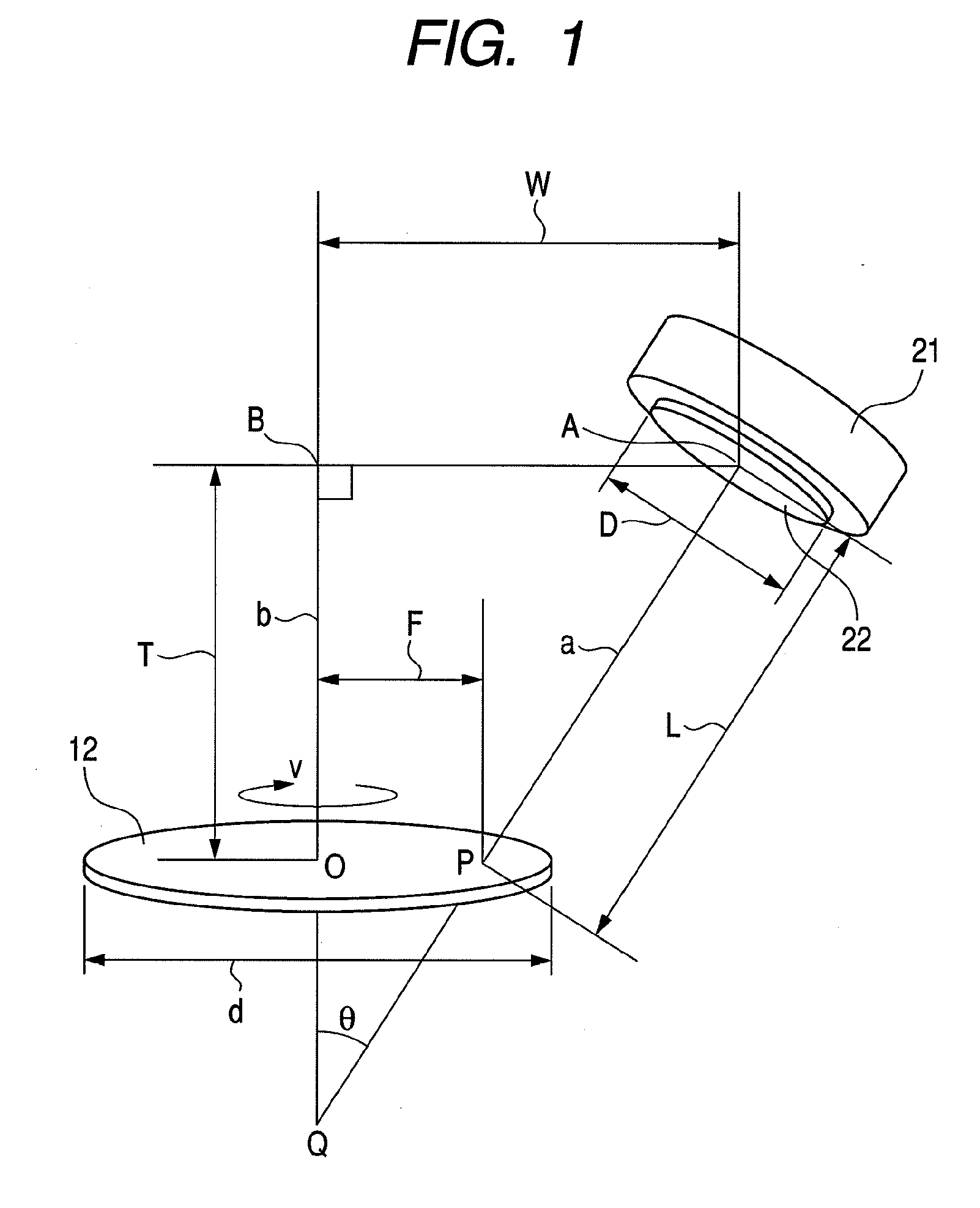
[0098]The first embodiment of the present invention will be described below referring to FIGS. 1 to 9. FIG. 1 illustrates the relative positioning of a target 22 and a substrate 12 of the sputtering apparatus to actualize the present invention. The symbol A is the center of surface of the target 22 placed on a target cathode 21. The symbol O is the center of surface of the substrate 12. The symbol B is the point of intersection between a normal to the surface of the substrate 12, including the center O of the substrate 12, and a line including the center A and being in parallel to the surface of the substrate 12. The symbol a is the normal to the surface of the target 22 passing through the center of the target or the center of the target cathode. The symbol b is the normal to the surface of the substrate 12 passing through the center of the substrate or the center of the substrate holder. The symbol 9 is the angle between the normal a and the normal b intersecting each other. The s...

example 2

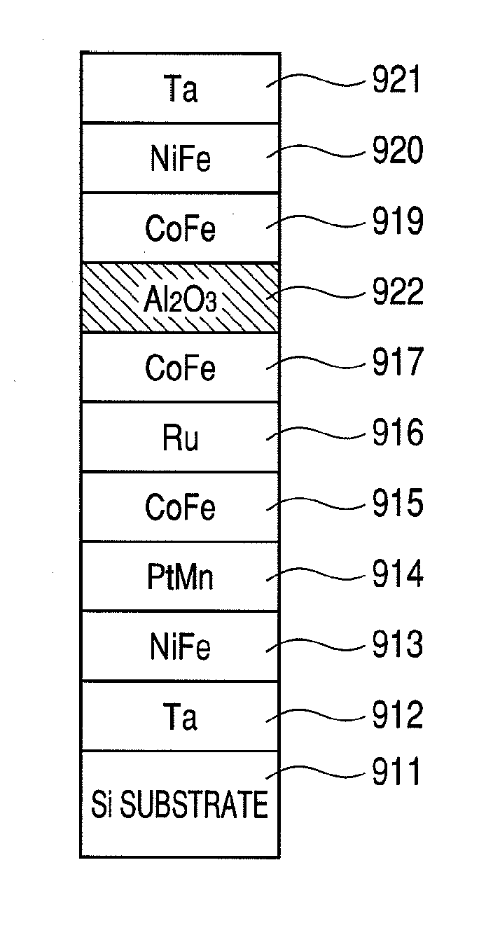
[0135]The second embodiment of the present invention will be described below referring to FIGS. 11 to 15. The second embodiment relates to forming an MTJ structure which is a magnetoresistive element used in MRAM and the like. Example 2 forms an MTJ having the structure illustrated in FIG. 12. The MTJ has a basic structure of a thin tunnel insulation film of about 1 nm in thickness and two thin magnetic films sandwiching the same. As a practical structure, the MTJ is made of a multilayer film composed of metallic films such as an antiferromagnetic layer to generate spin-valve action, an underlayer, and a protective layer. For the spin-valve action, detail description is given in, for example, “Magnetoresistive Head and Spin-Valve Head: 2nd Edition, Fundamental and Application” John C. Malinson, (translated by Kazuhiko Hayashi), Maruzen, (2002).

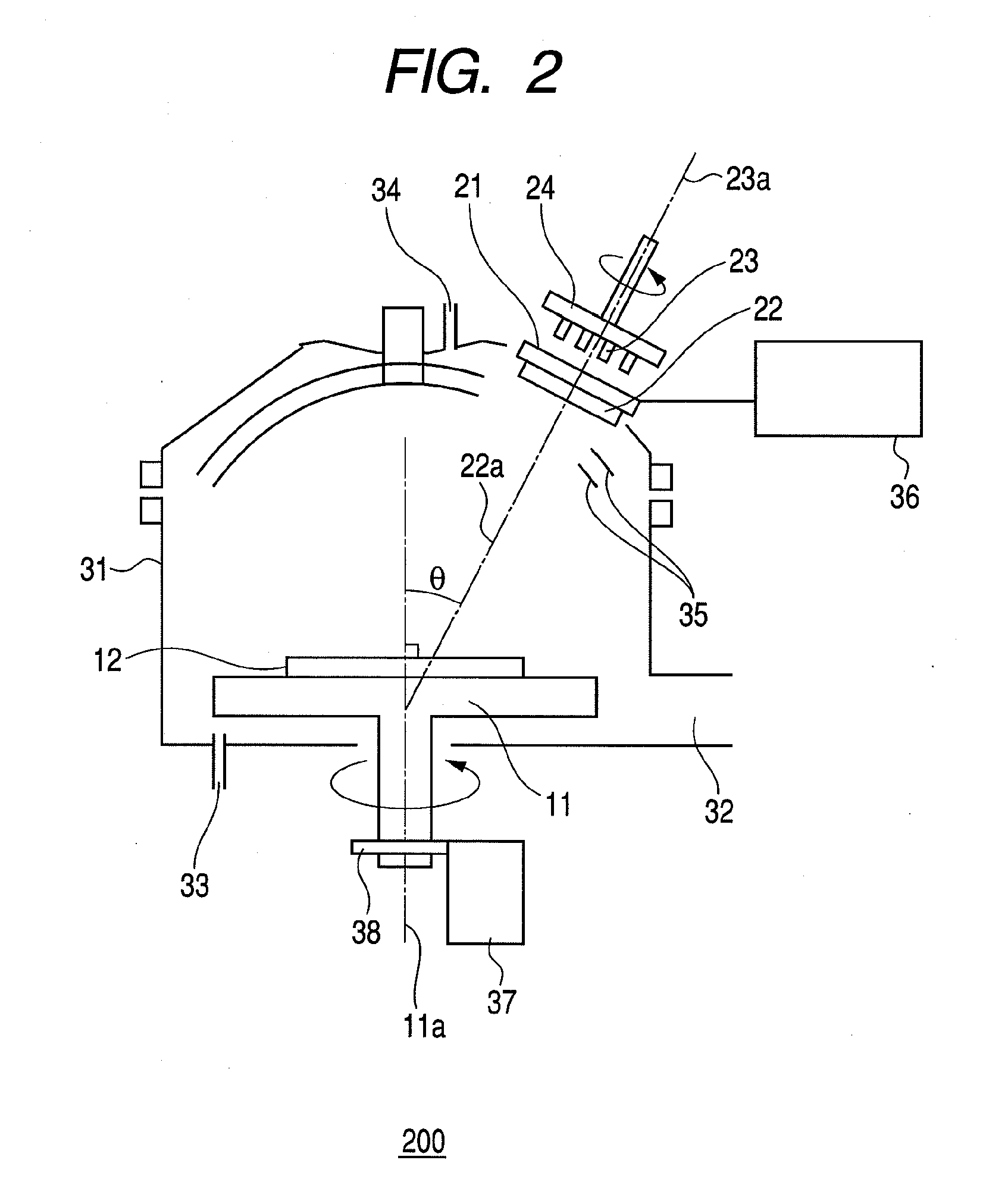
[0136]FIG. 11 is a schematic drawing illustrating the structure of a multi-chamber 1100 in Example 2, mounting the sputtering apparatus of th...


PUM

PropertyMeasurementUnit
thicknessaaaaaaaaaa
distanceaaaaaaaaaa
thicknessaaaaaaaaaa

Abstract

A sputtering method and a sputtering apparatus are provided in which a target is disposed being inclined relative to a substrate placed on a substrate-placing table so that the condition of d≧D is satisfied, (d is the diameter of the substrate, and D is the diameter of the target), and the total number of rotations R of the substrate-placing table from the beginning of film-deposition on the substrate to the completion thereof becomes ten or more. Also the sputtering method and the sputtering apparatus are provided in which the rotational speed V of the substrate-placing table is controlled so that the total number of rotations R thereof satisfies the formula of
0.95×S−0.025≦R≦1.05×S+0.025
at R≦10, (R is the total number of rotations of the substrate-placing table from the beginning of film-deposition on the substrate to the completion thereof, and S is the value of the number of total rotations R rounded off to integer).

Description

CROSS-REFERENCES TO RELATED APPLICATIONS[0001]This application is a continuation application of International Application No. PCT / JP2007 / 067484, filed on Sep. 7, 2007, the entire contents of which are incorporated by reference herein.BACKGROUND OF THE INVENTION[0002]1. Field of the Invention[0003]The present invention relates to a manufacturing method and a manufacturing apparatus to deposit an insulation film and a metal film, in the process of manufacturing a semiconductor device, to achieve high production yield of semiconductor elements and magnetoresistive elements at both intraplane and interplane of substrate through the deposition of the film having very thin and uniform thickness, and also relates to a semiconductor device. Specifically the present invention relates to a manufacturing method and a manufacturing apparatus for thinning a high-dielectric-constant film and for improving the performance of interface between the high-dielectric-constant film and a metal electrode...

Claims


Application Information

Patent Timeline
Patent Type & Authority Applications(United States)
IPC IPC(8): C23C14/36
CPCC23C14/165C23C14/225C23C14/34C23C14/505C23C14/568H01L21/28088H01L43/12H01L21/3144H01L21/318H01L29/4966H01L29/513H01L29/518H01L21/28229H01L21/02266H01L21/02183H01L21/02189H01L21/02192H01L21/02175H01L21/02178H01L21/02181H01L21/02186H10N50/01
Inventor MASHIMO, KIMIKOKITANO, NAOMUTSUNEKAWA, KOJI
Owner CANON ANELVA CORP
Why Eureka
Try Eureka