ZnO-BASED SUBSTRATE AND METHOD OF TREATING ZnO-BASED SUBSTRATE

a technology of zno-based substrate and zno-based substrate, which is applied in the field of zno-based substrate and the treatment method of zno-based substrate, can solve the problems of inability to achieve device configurations to satisfy required functions, lack of breakdown voltage capability in a high electric field, and inability to operate in a high voltage field, so as to prevent the production of zn hydroxide, reduce the crystal defect density of any of these thin films

Inactive Publication Date: 2010-06-03
ROHM CO LTD
View PDF3 Cites 8 Cited by
  • Summary
  • Abstract
  • Description
  • Claims
  • Application Information

AI Technical Summary

Benefits of technology

[0019]A ZnO-based substrate of the present invention is formed in a way that almost no OH groups exist on a crystal growth-side surface. Accordingly, it is possible to prevent production of a hydroxide of Zn. Moreover, when a ZnO thin film or a MgZnO thin film is formed on the ZnO-based substrate, it is possible to reduce a crystal defect density of any of these thin films to an extremely low level. Further, as the hydroxide of Zn is not produced, it is also possible to reduce adhesion of particles of silica and the like, and thereby to form a surface suitable for crystal growth.
[0020]Meanwhile, by applying an acidic wet etching process pH 3 or lower as a final process on a surface of a ZnO-based substrate, it is possible to eliminate almost all OH groups from the crystal growth-side surface. Hence, an effect similar to the above-described effect is achieved. Moreover, since it is possible to set the zeta potentials of ZnO and particles of silica or the like to the same polarity by the above-described etching, it is possible to further suppress generation of adhesion.

Problems solved by technology

In recent years, however, it is becoming more difficult to achieve device configurations to satisfy required functions due to property limitations of silicon materials themselves.
Such limitations include operational incapability at high temperature equal to or above 150° C. and lack of breakdown voltage capability in a high electric field, for example.
However, a sapphire substrate has a large degree of lattice mismatch with ZnO as the thin film material, which accounts for as high as about 18%.
For this reason, a conventional thin film is likely to have numerous lattice defects, an increase in mosaicness, and the like, and therefore it has been difficult to form a high-quality single-crystal thin film.
Therefore, a device, which is formed of a ZnO thin film deposited on a sapphire substrate, is incapable of fully exerting intrinsic performances of ZnO.
Hence, the sapphire substrate is not always the most suitable substrate for growth.
However, a ScAlMgO4 substrate is a special substrate which is not suitable for industrial applications without modifications.

Method used


Image

  • ZnO-BASED SUBSTRATE AND METHOD OF TREATING ZnO-BASED SUBSTRATE
  • ZnO-BASED SUBSTRATE AND METHOD OF TREATING ZnO-BASED SUBSTRATE
  • ZnO-BASED SUBSTRATE AND METHOD OF TREATING ZnO-BASED SUBSTRATE

Examples


example 1

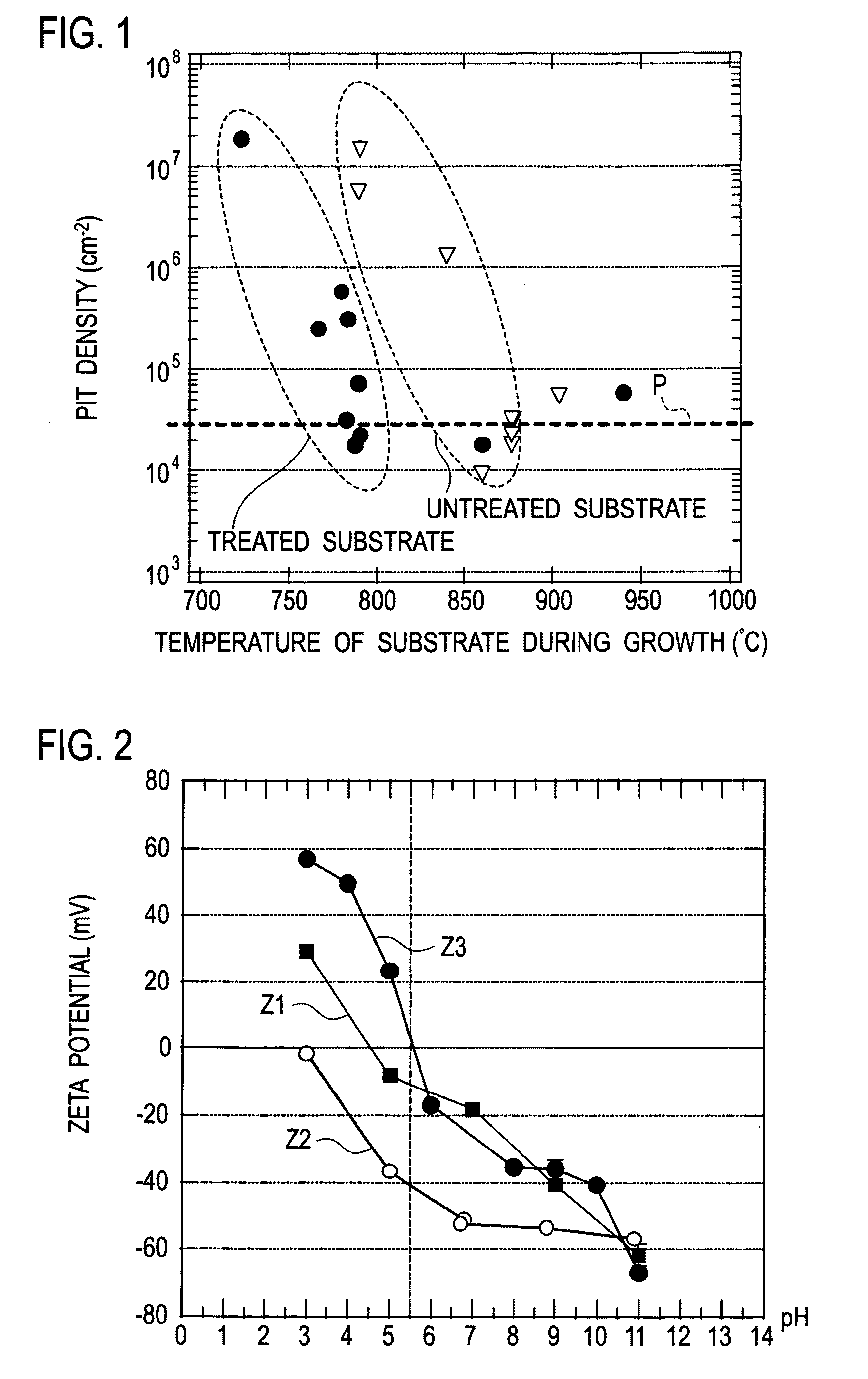
[0061]First, the main surface of the ZnO substrate is subjected to polishing by using colloidal silica to obtain a surface having a stepped structure including one to two molecular layers. If there is a significant process damage at this stage, removal etching for a damaged layer is subsequently executed by using an acid having the pH equal to or below 1. Thereafter, Zn(OH)2 is removed by etching using an acid having the pH set in a range of 2±0.5.

example 2

[0062]First, the main surface of the ZnO substrate is subjected to polishing by using colloidal silica to obtain a surface having a stepped structure including one to two molecular layers. If there is a significant process damage at this stage, etching is executed by using an acid having the pH equal to or below 1 and then etching is executed by using an acid containing fluorine and having the pH set in a range of 3.5±1 to dissolve silica on the ZnO substrate. Finally, etching is executed by using an acid having the pH set in a range of 2±0.5.

example 3

[0063]First, the main surface of the ZnO substrate is subjected to polishing by using colloidal silica to obtain a surface having a stepped structure including one to two molecular layers. If there is not a significant process damage at this stage, etching is executed by using an acid having the pH equal to or below 3. A time period for this etching varies depending on the pH but it is necessary to spend at least 15 second or longer.

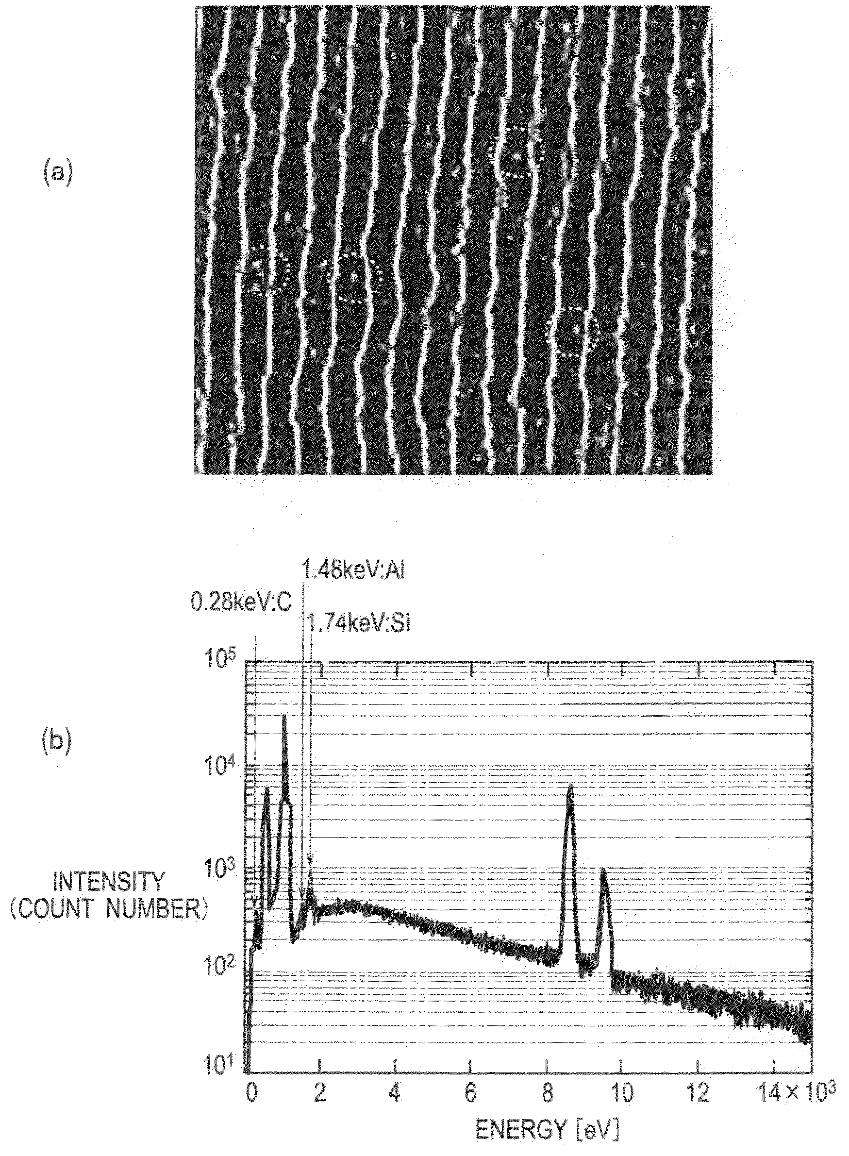
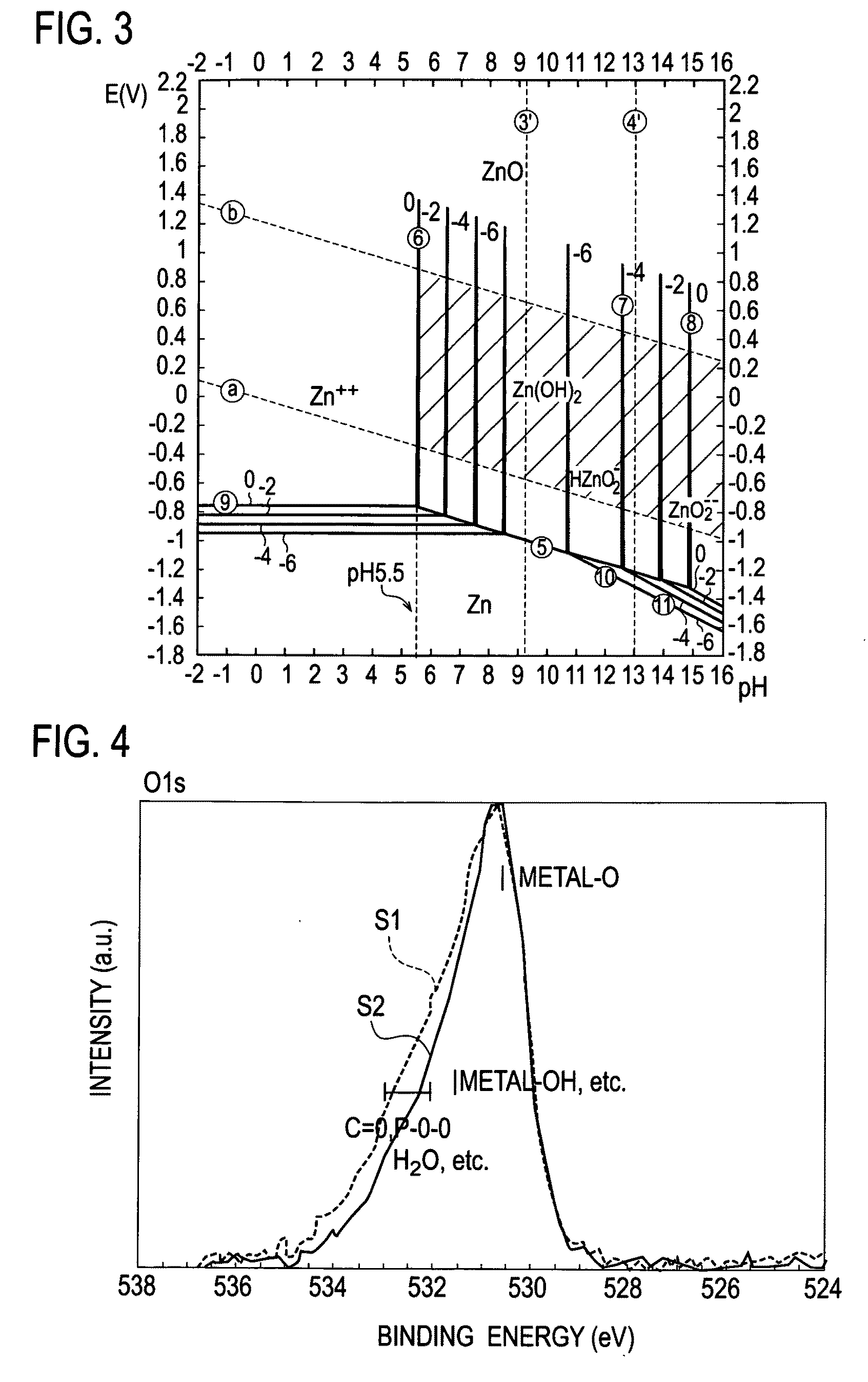
[0064]In any of the above-described examples, reduction of the OH groups is confirmed as shown in FIG. 4.


PUM

PropertyMeasurementUnit
pHaaaaaaaaaa
temperatureaaaaaaaaaa
diametersaaaaaaaaaa

Abstract

Provided are a ZnO-based substrate having a surface suitable for crystal growth, and a method of manufacturing the ZnO-based substrate. The ZnO-based substrate is made in a way that almost no hydroxide groups exist on a crystal growth-side surface of a MgxZn1-xO substrate (0≦x<1). To this end, as a method of treating the substrate, a final treatment to be applied on the crystal growth-side surface of the MgxZn1-xO substrate (0≦x<1) is acidic wet etching at pH 3 or lower. Thereby, it is possible to prevent production of a hydroxide of Zn, and to reduce the density of crystal defects in a thin film formed on the ZnO-based substrate.

Description

TECHNICAL FIELD[0001]The present invention relates to a ZnO-based substrate suitable for crystal growth of a ZnO-based thin film and the like, and to a method of treating the ZnO-based substrate.BACKGROUND ART[0002]Electronics engineering is a field where semiconductor materials, particularly silicon materials, play an active role. In recent years, however, it is becoming more difficult to achieve device configurations to satisfy required functions due to property limitations of silicon materials themselves. Such limitations include operational incapability at high temperature equal to or above 150° C. and lack of breakdown voltage capability in a high electric field, for example.[0003]In the meantime, oxides and organic materials represented by high-temperature superconductor YBCO, an ultraviolet-emitting material ZnO, an organic EL and the like are drawing attention as next generation materials owing to a variety of species and functional versatility. These substances have a possi...

Claims


Application Information

Patent Timeline
Patent Type & Authority Applications(United States)
IPC IPC(8): C09K11/54C23F1/00
CPCC30B29/16C30B35/007C30B33/10
Inventor NAKAHARA, KENYUJI, HIROYUKIAKASAKA, SHUNSUKEKAWASAKI, MASASHIOHTOMO, AKIRATSUKAZAKI, ATSUSHI
Owner ROHM CO LTD
Why Eureka
Try Eureka