Nonvolatile semiconductor memory device and method for manufacturing the same

a semiconductor memory and non-volatile technology, applied in the direction of semiconductor devices, basic electric elements, electrical appliances, etc., can solve the problems of varying the threshold voltage of the cell transistor, reducing the operating speed of the cell transistor constituting the memory cell,

Active Publication Date: 2010-06-10
KIOXIA CORP
View PDF4 Cites 320 Cited by
  • Summary
  • Abstract
  • Description
  • Claims
  • Application Information

AI Technical Summary

Problems solved by technology

However, in this manufacturing method, the silicon pillar is formed by depositing silicon on the tunnel insulating film.
Hence, microscopic structural defects at the atomic level are generated at high density at the interface between the tunnel insulating film and the silicon pillar, and this structural defect forms an interface state or a fixed charge.
This decreases the operating speed of the cell transistor constituting the memory cell.
Furthermore, the threshold voltage of the cell transistor varies after prolonged operation and causes malfunctions.

Method used


Image

  • Nonvolatile semiconductor memory device and method for manufacturing the same
  • Nonvolatile semiconductor memory device and method for manufacturing the same
  • Nonvolatile semiconductor memory device and method for manufacturing the same

Examples


first embodiment

[0017]At the outset, the invention is described.

[0018]FIGS. 1A and 1B to 6A and 6B illustrate a method for manufacturing a nonvolatile semiconductor memory device according to this embodiment, where each figure with the suffix A is a process cross-sectional view, and each figure with the suffix B is a process plan view.

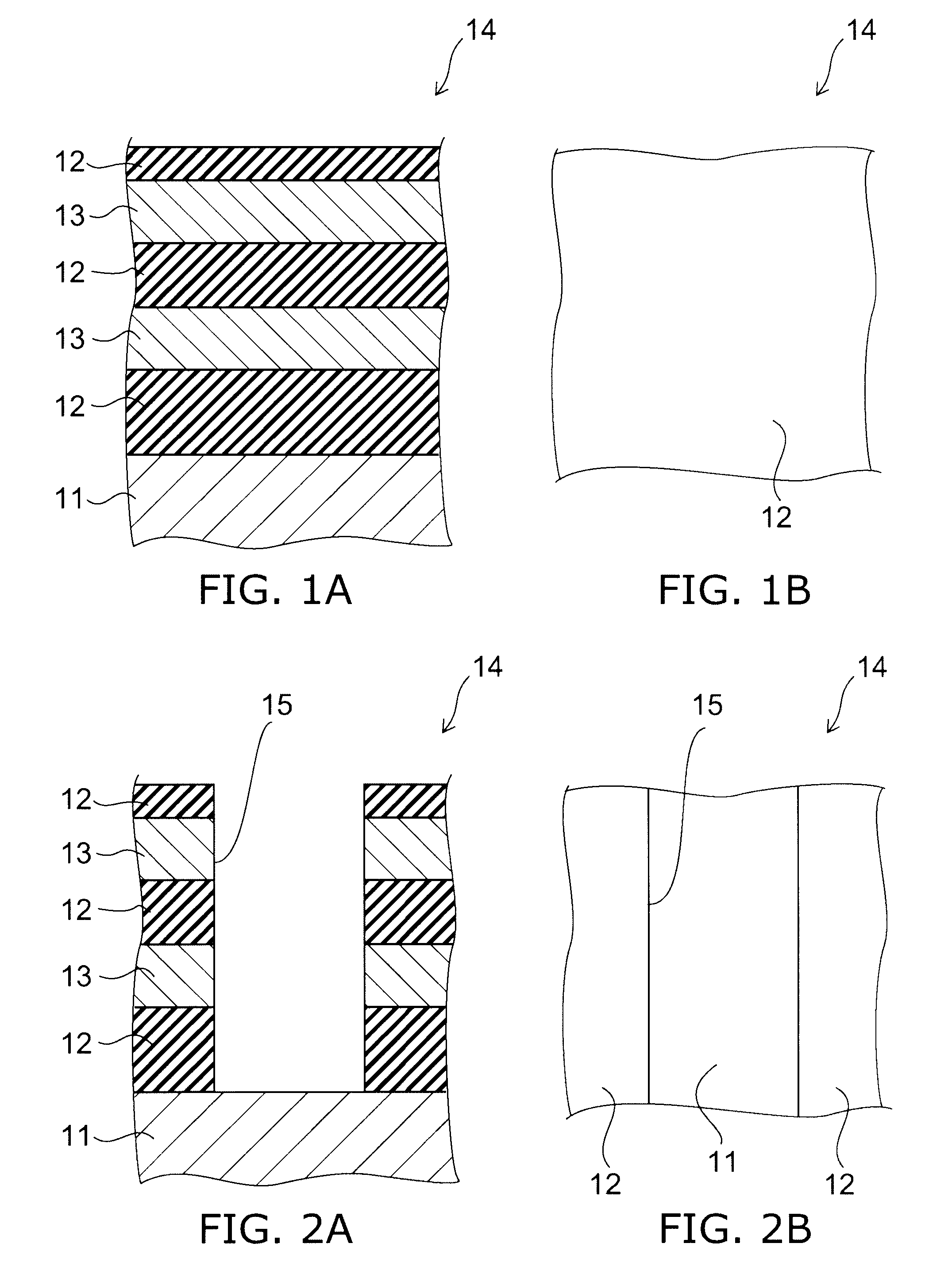
[0019]First, as shown in FIGS. 1A and 1B, on a silicon substrate 11, illustratively by the CVD process, silicon oxide films 12 to serve as interlayer insulating films and impurity-doped silicon films 13 to serve as gate electrodes are alternately deposited to form a multilayer body 14. The thickness of the silicon oxide film 12 and the silicon film 13 is e.g. 50 nm (nanometers) each. Although FIG. 1A shows only two silicon films 13, this embodiment is not limited thereto. The number of silicon films 13 is arbitrary.

[0020]Next, as shown in FIGS. 2A and 2B, a resist mask (not shown) is formed on the stacked body 14 and used as a mask to perform RIE (reactive ion etching...

second embodiment

[0033]Next, the invention is described.

[0034]FIGS. 7A and 7B to 8A and 8B are process cross-sectional views illustrating a method for manufacturing a nonvolatile semiconductor memory device according to this embodiment, where each figure with the suffix B is a partially enlarged view of region R shown in the corresponding figure with the suffix A.

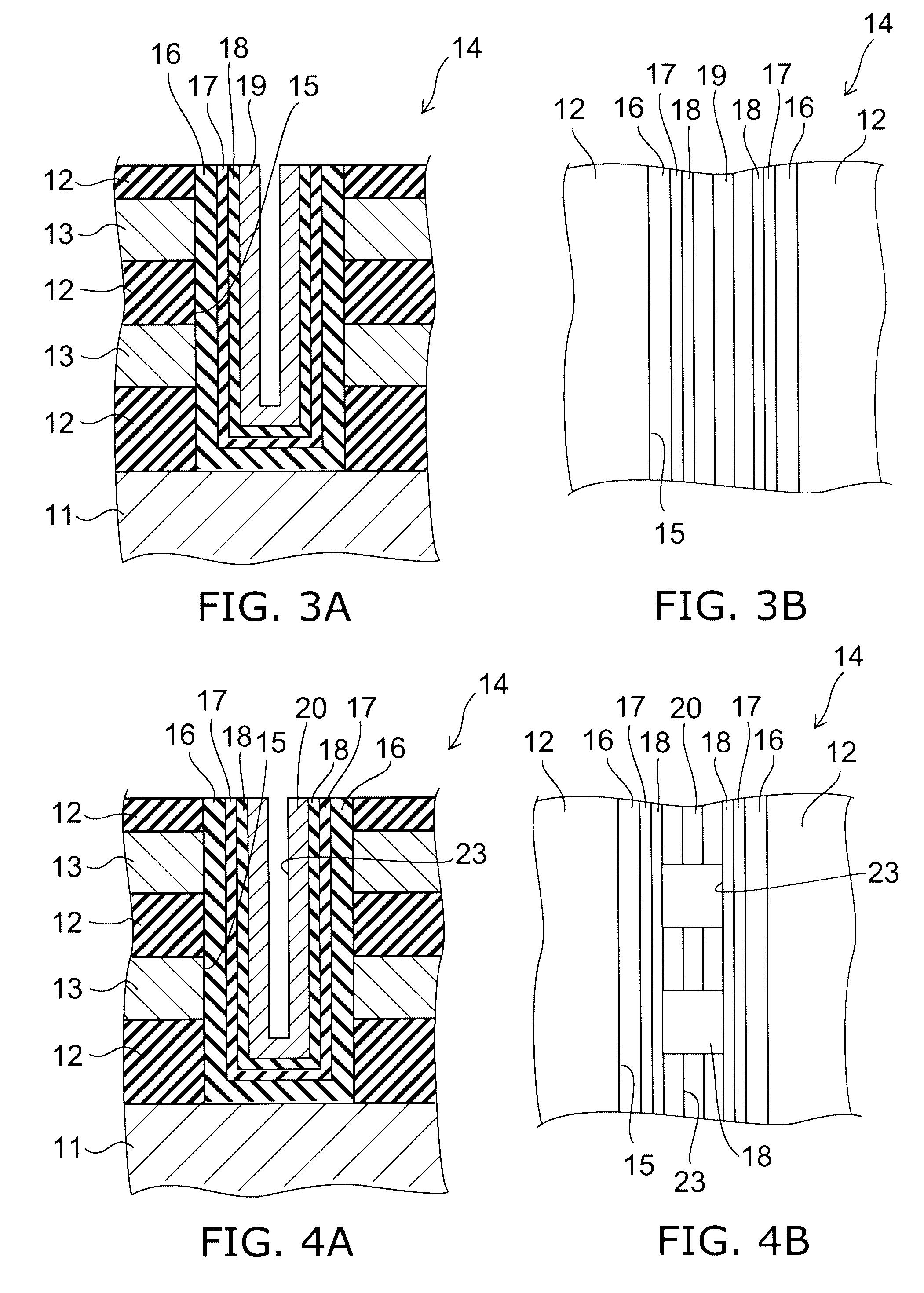
[0035]First, by a method similar to that in the above first embodiment, a structure shown in FIGS. 4A and 4B is fabricated. Next, as shown in FIG. 7A, thermal oxynitridation is performed in a nitrogen monoxide gas (NO) atmosphere. The condition for this thermal oxynitridation is such that the temperature is e.g. 700 to 1200° C. and the duration is e.g. 1 minute to 1 hour. Here, the nitrogen monoxide gas atmosphere is not limited to an atmosphere containing only nitrogen monoxide gas, but can be any atmosphere containing nitrogen monoxide gas.

[0036]By this thermal oxynitridation, a silicon oxynitride layer 24a having a thickness of e.g. appr...

third embodiment

[0045]Next, the invention is described.

[0046]FIGS. 9A and 9B to 14A and 14B illustrate a method for manufacturing a nonvolatile semiconductor memory device according to this embodiment, where each figure with the suffix A is a process cross-sectional view, and each figure with the suffix B is a process plan view.

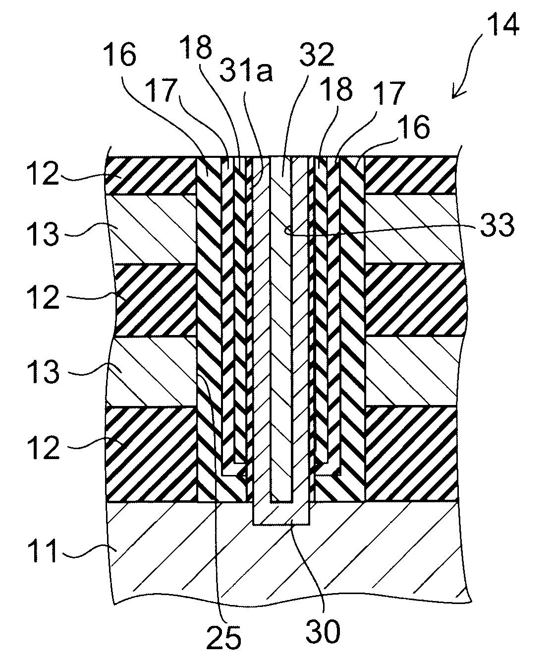
[0047]This embodiment is different from the above first embodiment in that the trench is shaped like a cylinder rather than a groove, and that the channel silicon crystal layer is extended to the silicon substrate.

[0048]First, as shown in FIGS. 9A and 9B, by a method similar to that in the above first embodiment, a stacked body 14 is formed on a silicon substrate 11.

[0049]Next, as shown in FIGS. 10A and 10B, RIE is performed using a resist mask (not shown) to form a plurality of trenches 25 in the stacked body 14. The trench 25 is shaped like a cylinder extending in the stacking direction of the stacked body 14, and its inner diameter is e.g. 70 nm. As viewed in the stacking...


PUM

PropertyMeasurementUnit
temperatureaaaaaaaaaa
thicknessaaaaaaaaaa
widthaaaaaaaaaa

Abstract

On a silicon substrate is formed a stacked body by alternately stacking a plurality of silicon oxide films and silicon films, a trench is formed in the stacked body, an alumina film, a silicon nitride film and a silicon oxide film are formed in this order on an inner surface of the trench, and a channel silicon crystalline film is formed on the silicon oxide film. Next, a silicon oxide layer is formed at an interface between the silicon oxide film and the channel silicon crystalline film by performing thermal treatment in an oxygen gas atmosphere.

Description

CROSS-REFERENCE TO RELATED APPLICATIONS[0001]This application is based upon and claims the benefit of priority from the prior Japanese Patent Application No. 2008-314187, filed on Dec. 10, 2008; the entire contents of which are incorporated herein by reference.BACKGROUND OF THE INVENTION[0002]1. Field of the Invention[0003]This invention relates to a nonvolatile semiconductor memory device in which a channel film made of silicon is formed on an insulating film, and a method for manufacturing the same.[0004]2. Background Art[0005]Recently, as an alternative to the planar nonvolatile semiconductor memory device, a nonvolatile semiconductor memory device in which a plurality of MONOS (metal-oxide-nitride-oxide-silicon) type memory cells are three-dimensionally stacked has been developed (see, e.g., JP-A-2008-171918(Kokai)). This nonvolatile semiconductor memory device is manufactured as follows. Gate electrodes and interlayer insulating films are alternately formed on a substrate to fo...

Claims


Application Information

Patent Timeline
Patent Type & Authority Applications(United States)
IPC IPC(8): H01L29/792H01L21/28H01L21/20
CPCH01L21/28282H01L27/11582H01L29/0657H01L29/4234H01L21/02667H01L29/792H01L29/7926H01L21/02255H01L29/66833H01L29/40117H10B43/27H10B99/00
Inventor OZAWA, YOSHIO
Owner KIOXIA CORP
Why Eureka
Try Eureka