Semiconductor Device and Fabricating Method Thereof

a technology of semiconductor devices and semiconductors, applied in semiconductor devices, inductances, electrical devices, etc., to achieve the effect of reducing parasitic capacitan

Inactive Publication Date: 2010-06-10
DONGBU HITEK CO LTD
View PDF1 Cites 12 Cited by
  • Summary
  • Abstract
  • Description
  • Claims
  • Application Information

AI Technical Summary

Benefits of technology

[0011]Accordingly, exemplary embodiments of the present invention are directed to solving the above conventional problem, and provide an inductor

Problems solved by technology

Here, the inductor is a single device occupying the greatest space in a chip and may be limited with regard to high frequency ch

Method used


Image

  • Semiconductor Device and Fabricating Method Thereof
  • Semiconductor Device and Fabricating Method Thereof
  • Semiconductor Device and Fabricating Method Thereof

Examples


Embodiment Construction

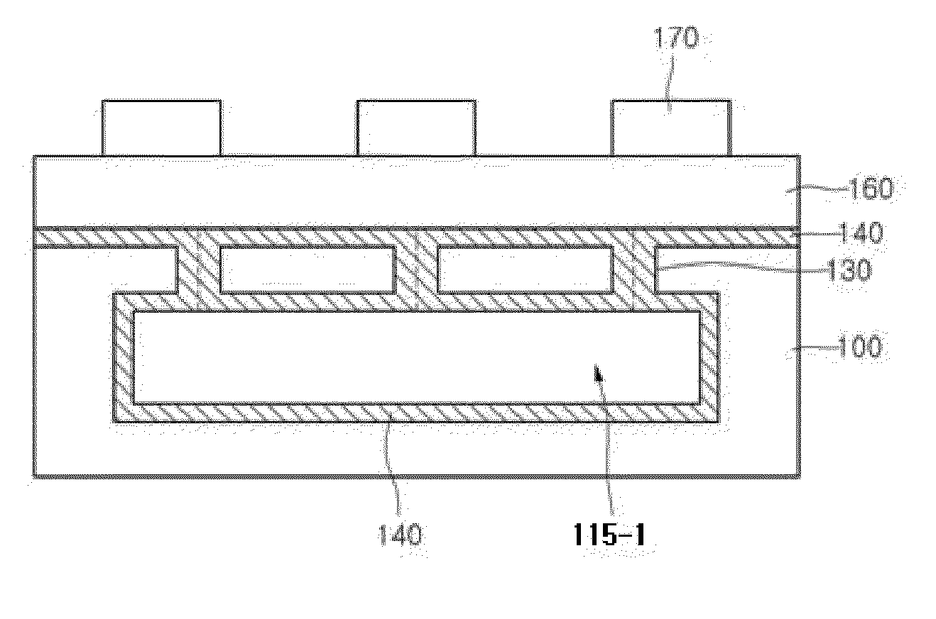
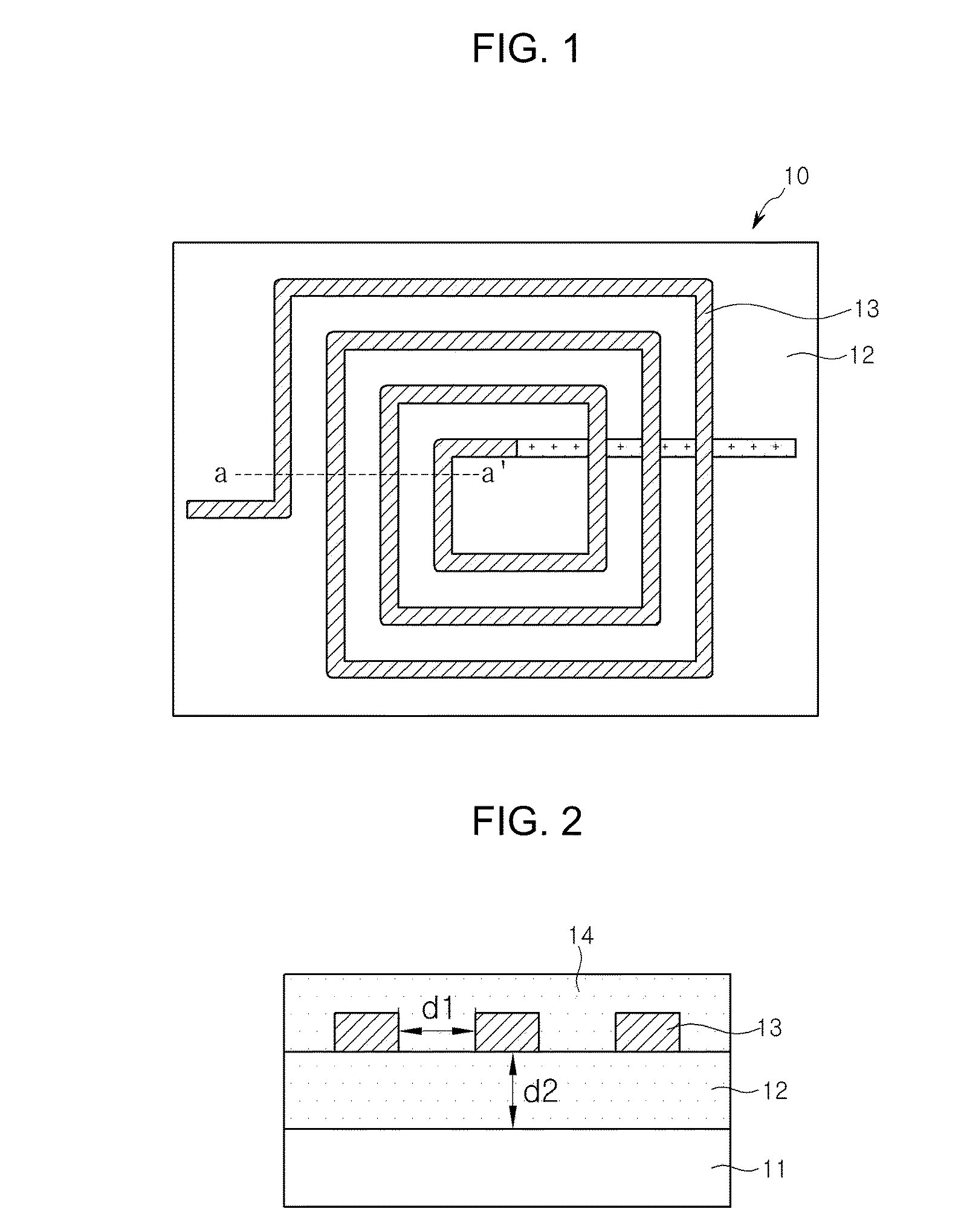
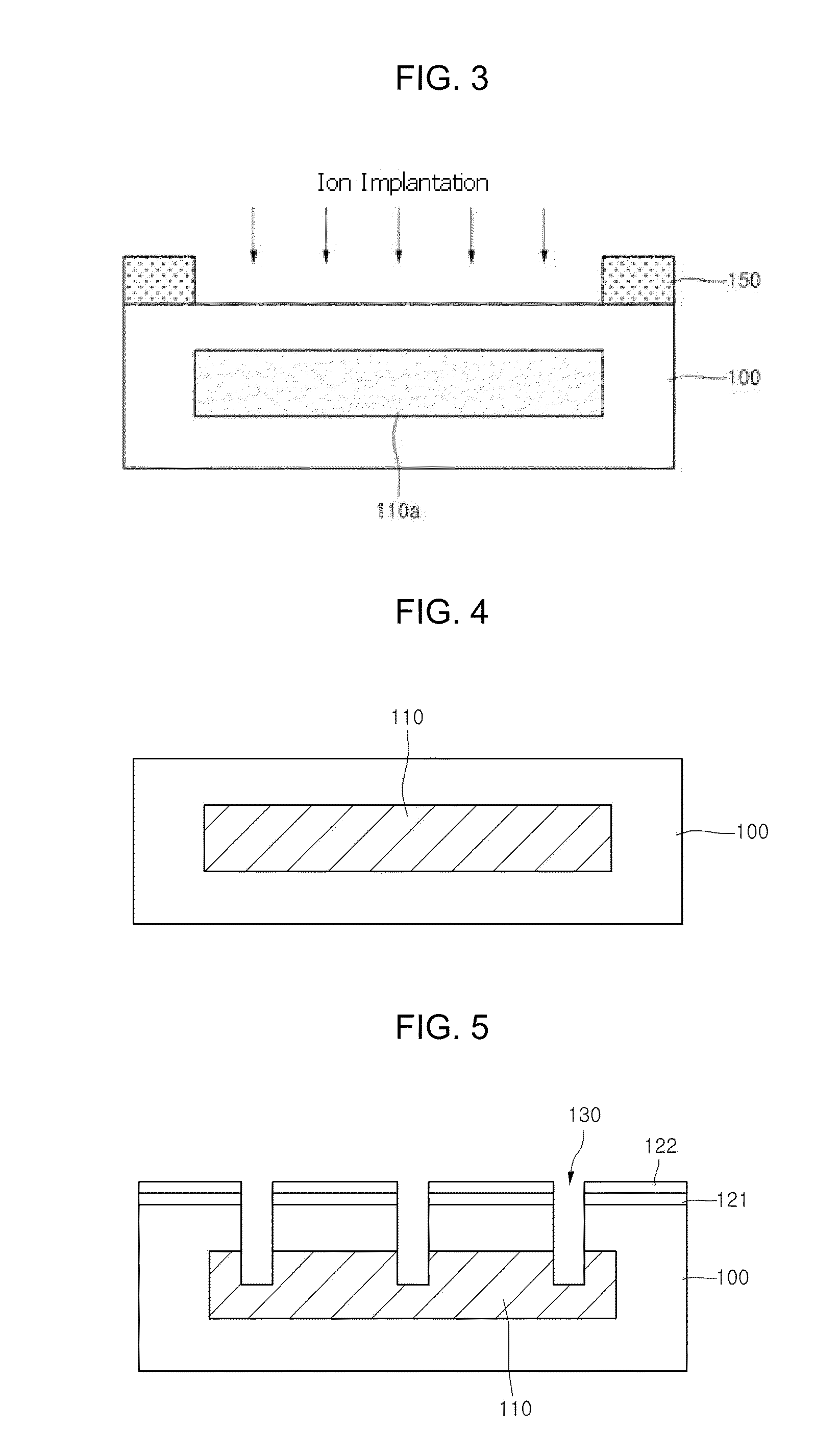
[0023]Hereinafter, a semiconductor device and a process for manufacturing the same will be described in detail from the following description with reference to exemplary embodiments, taken in conjunction with the accompanying drawings. Hereinafter, “first,”“second,” etc. are used to distinguish individual components without restriction thereof and mean that at least two components are provided. Accordingly, if “first,”“second,” etc. are mentioned, it is clearly understood that a plurality of components are provided in the foregoing semiconductor device and respective components are selectively used or mutually exchangeable. In addition, a size (dimension) of each component shown in the figures is enlarged for more detailed understanding of the invention and a ratio of sizes between components shown in the figures may be different from a ratio of actual sizes between the same components. All of the components shown in the figures need not either be included in the present invention o...


PUM


Abstract

Disclosed is a semiconductor device which includes a substrate having an air layer or void therein, an interlayer dielectric film above the substrate, and a metal wiring having a spiral structure on the interlayer dielectric film corresponding to or over the air layer. The semiconductor device exhibits reduced parasitic capacitance between the metal wiring (used as an inductor) and the substrate, thereby improving a self-resonance frequency as well as an applicable frequency band of the inductor.

Description

[0001]This application claims the benefit of Korean Patent Application No. 10-2008-0122793, filed on Dec. 4, 2008, which is hereby incorporated by reference as if fully set forth herein.BACKGROUND OF THE INVENTION[0002]1. Field of the Invention[0003]Exemplary embodiments of the present invention relate to a semiconductor device and a method for fabrication thereof.[0004]2. Discussion of the Related Art[0005]With development of micro-processing technologies, complementary metal-oxide semiconductor (“CMOS”) technologies with improved frequency characteristics have been proposed. Applying semiconductor processing techniques makes fabrication of chips economically feasible. In particular, since immediate frequency (“IF”) circuits and digital circuits can also be integrated into a chip, a System on Chip (“SOC”) process is increasingly attracting attention as an appropriate technology for fabrication of single chips in the related art.[0006]An RF-CMOS or bipolar / BiCMOS device includes an ...

Claims


Application Information

Patent Timeline
IPC IPC(8): H01L29/41H01L21/02
CPCH01L28/10H01L27/04
Inventor KIM, NAM JOO
Owner DONGBU HITEK CO LTD
Why Eureka
Try Eureka