Scanner model representation with transmission cross coefficients

a transmission cross coefficient and scanner model technology, applied in the field of simulating aspects of lithographic processes, can solve the problems of difficult to reproduce patterns on wafers, large cost of making high-end mask sets, and general inability to apply opc, etc., and achieve the effect of accuracy advantag

Active Publication Date: 2010-06-10
ASML NETHERLANDS BV
View PDF23 Cites 57 Cited by
  • Summary
  • Abstract
  • Description
  • Claims
  • Application Information

AI Technical Summary

Benefits of technology

[0022]The aspects of the invention allow a proper separation of concerns between the scanner vendor and the OPC vendor. All the details of scanner optics remain as knowledge and responsibility of the scanner vendor, without compromising the application of such data in OPC-type products. The encapsulation is achieved via a well-defined mathematical transform, i.e., the TCC calculation algorithm. Basic optical information such as illuminator shape and polarization, Jones pupil, focus blur due to laser bandwidth and / or chromatic aberrations, Jones pupil, etc., can be easily incorporated into the TCCs. Field-dependent effects such as through-slit variations can be captured by providing multiple TCCs, one for each field or slit position.
[0023]Imaging simulation can then performed by convolving the mask patterns with the TCC eigenvectors. The imaging simulation will enable the accuracy advantage of using scanner data in RET-type of applications such as OPC and OPC verification. With the addition of predictive scanner models such as pupil predictor, it will also enable process design applications such as SMO (source-mask optimization) and model-based scanner tuning. The invention thus helps protect sensitive information related to a scanner design, while at the same time enabling access to scanner data for the purpose of imaging simulations. Moreover, it helps contain the communication related to such data, including the descriptions, conventions, interpretations, and validations, within the manufacturer of the scanner. Further, it helps the proliferation of scanner data beyond products that exclusively use a particular type of scanner product.

Problems solved by technology

These rules are set by processing and design limitations.
In general, the smaller k1, the more difficult it becomes to reproduce a pattern on the wafer that resembles the shape and dimensions planned by a circuit designer in order to achieve particular electrical functionality and performance.
However, applying OPC is generally not an ‘exact science’, but an empirical, iterative process that does not always resolve all possible weaknesses on a layout.
This is driven by the enormous cost of making high-end mask sets, which run in the multi-million dollar range, as well as by the impact on turn-around time by reworking or repairing actual masks once they have been manufactured.
This requires a lot of knowledge transfer between the scanner vendor and the OPC vendor.
This process is error prone, and hinders continuous improvement of model accuracy.
This becomes a serious and burdensome data management problem.
Accurate scanner data and physical models enhance significantly the accuracy of the optical part of a CL model, but require in depth understanding of the corresponding subsystem functionality and are therefore not easy to use outside the range of their normally very narrow intended user base.
Furthermore, such models or data may not only expose an unnecessary level of detail, but also information that is proprietary and therefore cannot be made widely available.
Given the concerns discussed above, the goal of making scanner data available for model accuracy improvement would be inherently futile if it were just a best-effort without any means of actually ensuring model quality.
This overcomes the possibility that as soon as different TCC generation algorithms are applied to the same scanner data, the results would be immediately guaranteed to be different, making wide spread application quite unmanageable.

Method used


Image

  • Scanner model representation with transmission cross coefficients
  • Scanner model representation with transmission cross coefficients
  • Scanner model representation with transmission cross coefficients

Examples


Embodiment Construction

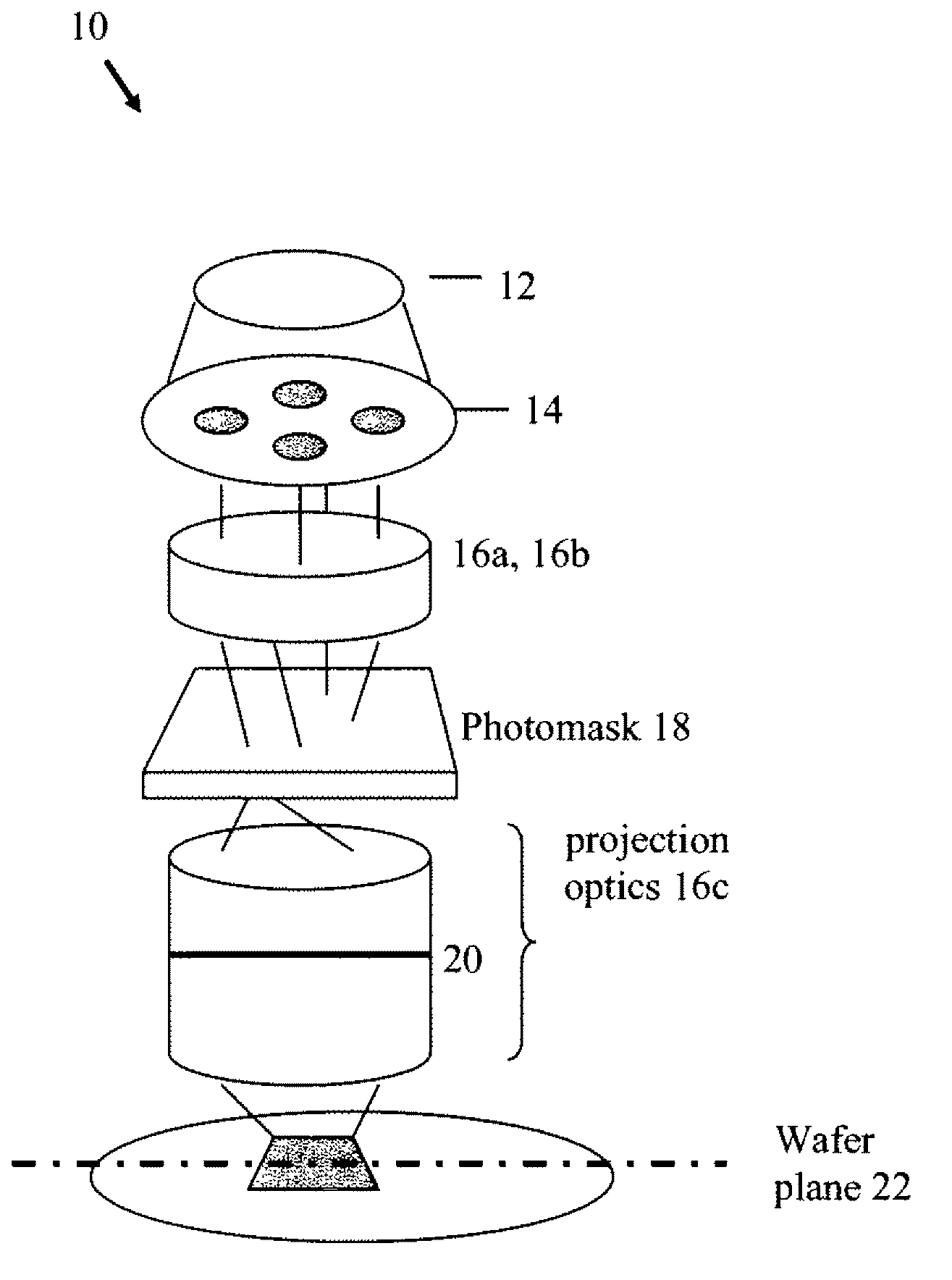
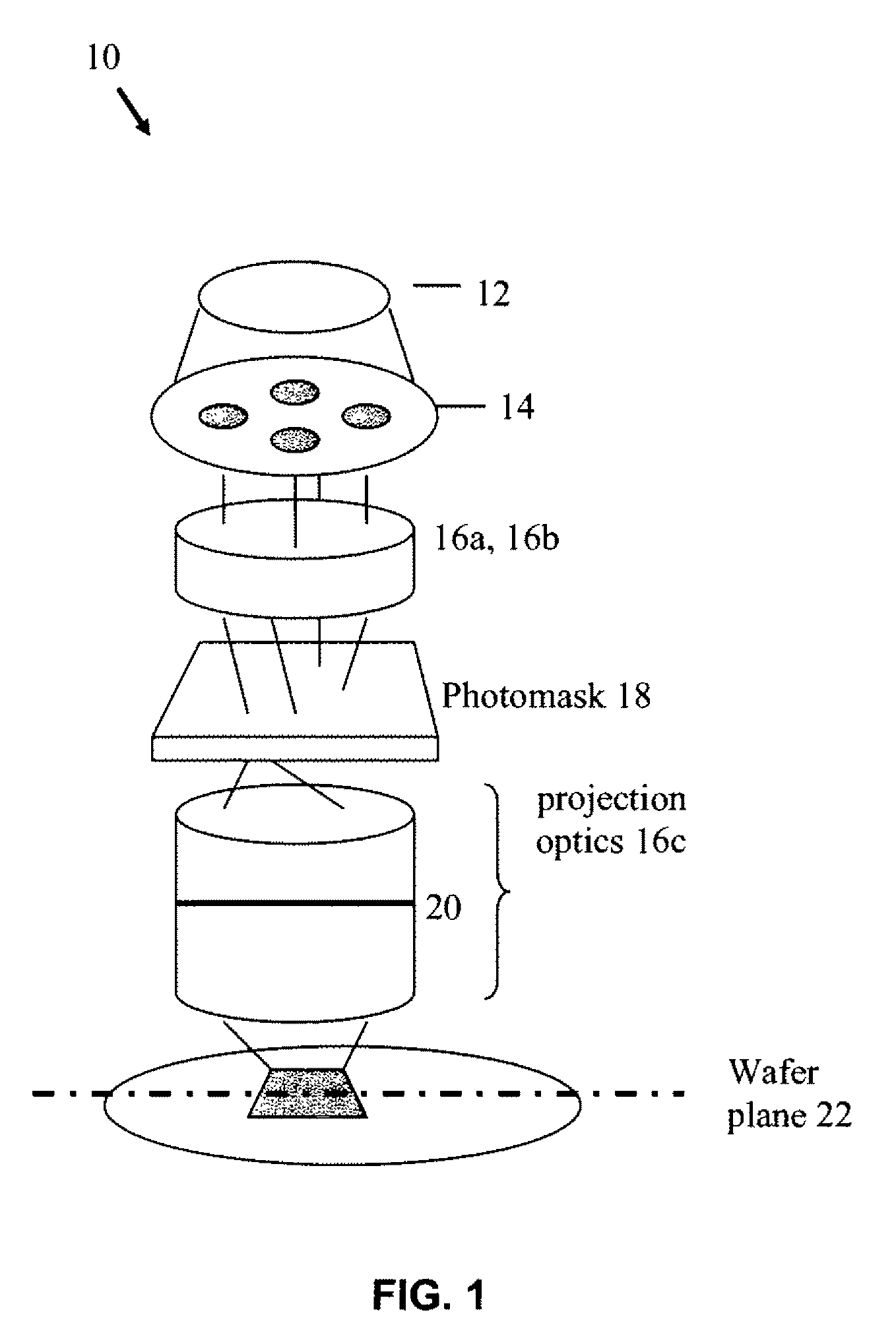
[0042]Prior to discussing the present invention, a brief discussion regarding the overall simulation and imaging process is provided. FIG. 1 illustrates an exemplary lithographic projection system 10. The major components are a light source 12, which may be a deep-ultraviolet excimer laser source, illumination optics which define the partial coherence (denoted as sigma) and which may include specific source shaping optics 14, 16a and 16b; a mask or reticle 18; and projection optics 16c that produce an image of the reticle pattern onto the wafer plane 22. An adjustable filter or aperture 20 at the pupil plane may restrict the range of beam angles that impinge on the wafer plane 22, where the largest possible angle defines the numerical aperture of the projection optics NA=sin(Θmax).

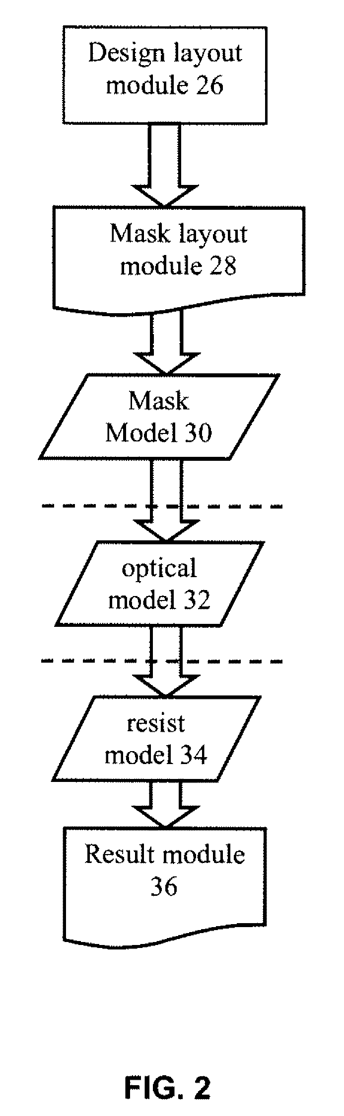
[0043]In a lithography simulation system, these major system components can be described by separate functional modules, for example, as illustrated in FIG. 2. Referring to FIG. 2, the functional modules i...


PUM


Abstract

The present invention relates to a method for simulating aspects of a lithographic process. According to certain aspects, the present invention uses transmission cross coefficients to represent the scanner data and models. According to other aspects, the present invention enables sensitive data regarding various scanner subsystems to be hidden from third party view, while providing data and models useful for accurate lithographic simulation.

Description

CROSS-REFERENCE TO RELATED APPLICATIONS[0001]The present application claims priority to U.S. Patent Appln. No. 61 / 112,913, filed Nov. 10, 2008, the contents of which are incorporated herein by reference in their entirety.FIELD OF THE INVENTION[0002]The present invention relates to a method for simulating aspects of a lithographic process.BACKGROUND OF THE RELATED ART[0003]Lithographic apparatuses can be used, for example, in the manufacture of integrated circuits (ICs). In such a case, the mask may contain a circuit pattern corresponding to an individual layer of the IC, and this pattern can be imaged onto a target portion (e.g. comprising one or more dies) on a substrate (silicon wafer) that has been coated with a layer of radiation-sensitive material (resist). In general, a single wafer will contain a whole network of adjacent target portions that are successively irradiated via the projection system, one at a time. In one type of lithographic projection apparatus, each target por...

Claims


Application Information

Patent Timeline
Patent Type & Authority Applications(United States)
IPC IPC(8): G03B27/32
CPCG03F7/705G03F7/70666G03F7/70508
Inventor CAO, YUYE, JUNKOONMEN, JAMES PATRICKHUNSCHE, SLEFAN
Owner ASML NETHERLANDS BV
Why Eureka
Try Eureka