

Method for Transferring a Nanolayer
a nanolayer and nanotechnology, applied in the field of nanolayer transfer, can solve the problems of not enabling a controlled transfer onto another substrate, all these layers can only obtain a technical relevance,
- Summary
- Abstract
- Description
- Claims
- Application Information
AI Technical Summary
Problems solved by technology
Method used
Image

Examples
example 1
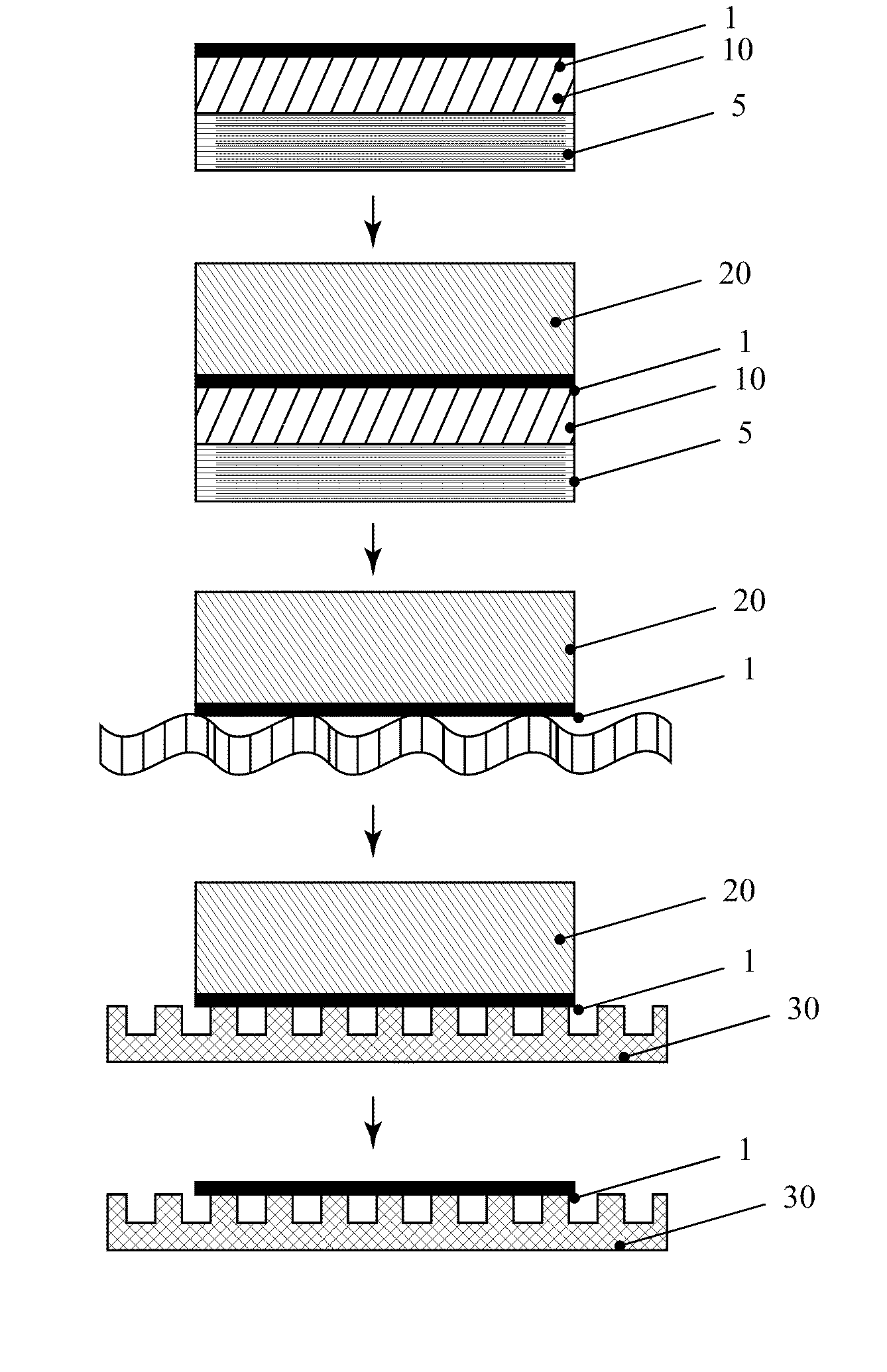
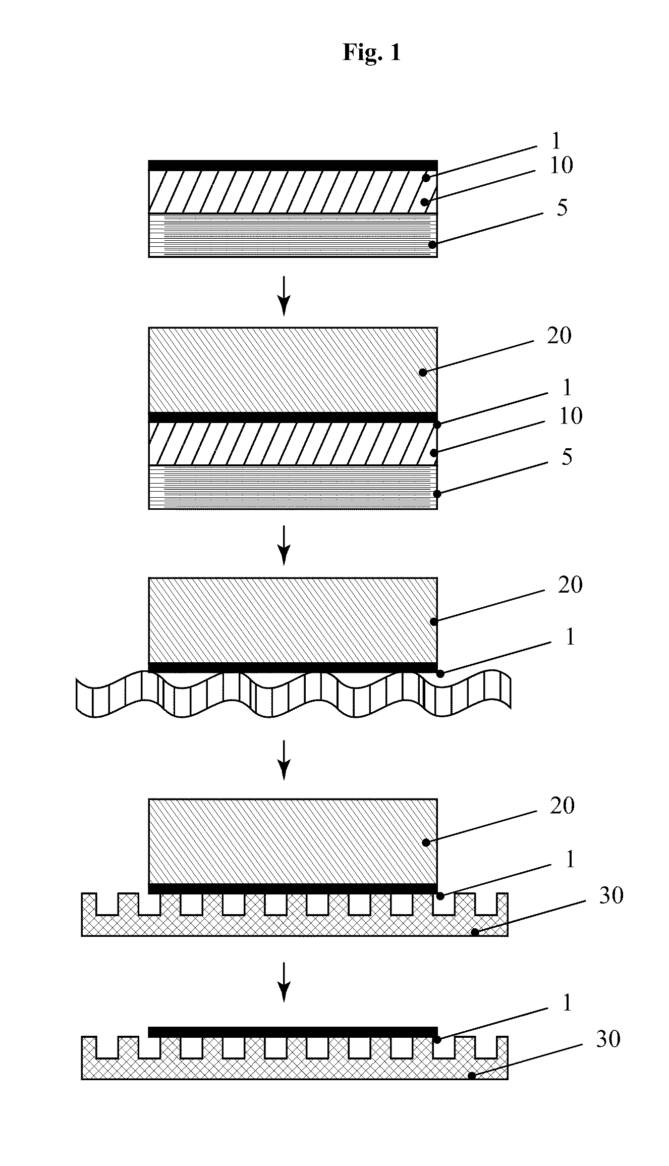
[0028]Transfer of a cross-linked monolayer of 4′-[(3-trimethoxysilyl) proproxy]-[1,1′-biphenyl]-4-carbonitril (in the following monolayer (I)) to a TEM grid. Such a monolayer has significant advantages for electron microscopy. The layer thickness is given by the length of the monomers from which the monolayer is formed. Therefore, it is to a large extent homogenous and is approximately 1.5 nm. Compared to this, conventional TEM substrates are significantly thicker leading to a less sample contrast in the TEM image. Chemical nano-lithography can be executed on the monolayer (I), cf. Biebricher A. et al.; Journal of Biotechnology 112, 97, (2004). With it, for example organic molecules can be bound on well defined positions onto the monolayer (I).
[0029]For the manufacture of the coated TEM grid the monolayer (I) is at first prepared on a silicon substrate coated with silicon nitride. The silicon is used in this example as carrier substrate; the silicon nitride layer serves as a sacrifi...
example 2
[0036]Transfer of a structured monolayer (I) to a gold substrate.
[0037]Nano-layers with self-aggregating monolayers (SAM) can be prepared on a number of substrates. For this purpose, a suitable SAM substrate combination has to be known. For example, the monolayer can be used as resist for wet chemical etching or for metal deposition. Furthermore, (bio-) molecules can be coupled by “chemical lithography”.
[0038]However, for a given substrate a suitable molecule is not always available to generate monolayers. In particular, a lot of effort is necessary to obtain a new SAM substrate combination and to characterize it. For lithographical processes it is in addition generally necessary that the substrate is plain.
[0039]With the inventive transfer of monolayers it is however possible to use known SAM substrate combinations the previous lithographical structuring can be made on a flat substrate. The transfer can then occur to curved surfaces as well as on substrates on which no SAM can be f...
example 3
[0042]Transfer of a 1,1′-biphenyl-4-thiol monolayer (in the following monolayer (II)) to a silicon oxide substrate.
[0043]In this example, the monolayer (II) is at first prepared on mica coated with gold. The mica serves as carrier substrate, the gold serves as sacrificial layer and the monolayer (II) is the monolayer to be transferred. As transfer medium a photoresists is used (for example AR-P 3510 of Allresist GmbH, www.allresist.de). The resist is spun onto the carrier substrate and hardened on a heating plate.
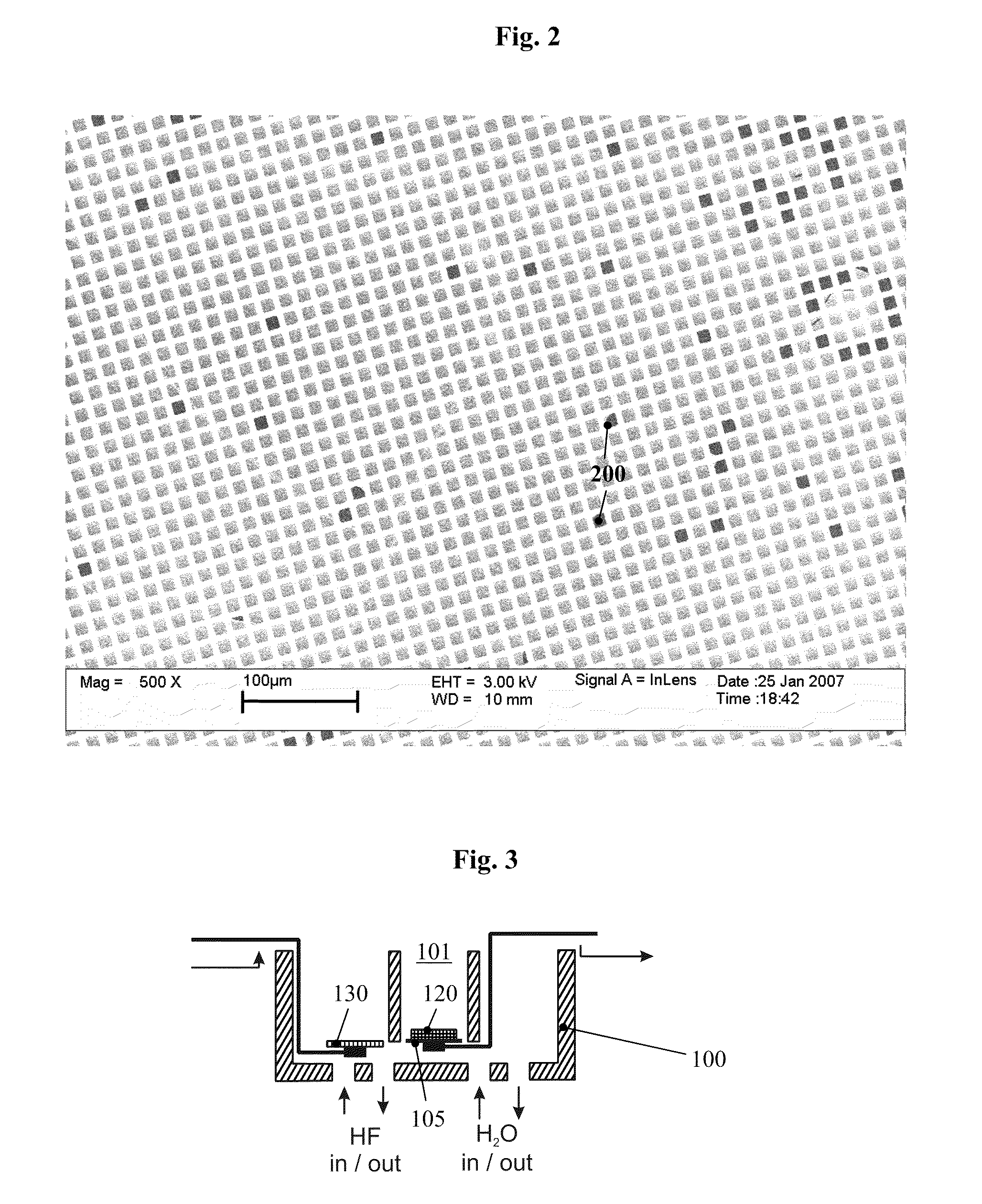
[0044]In the next step, the mica substrate is striped layer by layer with a tape (for example Scotch tape of 3M); alternatively it can be dissolved in hydrofluoric acid. Afterwards, the gold (sacrificial layer) is removed (for example with an iodine / potassium iodine solution or potassium cyanide solution) by allowing the sample to float on the etching solution. With a tweezers a silicon oxide sample can now be dipped into the solution, and thus the monolayer (II) with the p...
PUM
 Abstract
Description
Claims
Application Information