
Production method for electronic chip component

Active Publication Date: 2010-06-17
MURATA MFG CO LTD
View PDF2 Cites 20 Cited by
  • Summary
  • Abstract
  • Description
  • Claims
  • Application Information

AI Technical Summary

Benefits of technology

[0010]Accordingly, preferred embodiments of the present invention provide a production method for an electronic chip component that can easily produce electronic chip components with a high production yield.
[0015]Preferably, the paste is a conductive paste, and the first and second functional members are first and second external electrodes. In this case, it is possible to easily produce electronic ceramic chip components with a high production yield.
[0017]Preferably, a surface of the slider facing the first end surface has elasticity. This structure allows the electronic component body to be easily turned with high reliability. Further, this structure can effectively prevent the electronic component body from being damaged by contact with the slider.
[0018]Preferably, the slider includes a support member and an elastic member stuck onto a surface of the support member. This structure allows the surface of the slider to be kept flat. It is therefore possible to easily turn the electronic component body with high reliability. In addition, handlability of the slider can be improved.
[0020]Preferably, a surface of the slider facing the first end surface has irregularities. This structure allows the electronic component body to be easily turned with high reliability.
[0021]In the production method for the electronic chip component according to a preferred embodiment of the present invention, the electronic component body is turned by sliding the slider relative to the substrate in a state in which the slider is in contact with the first end surface of the electronic component body, thereby exposing the second end surface. Since it is unnecessary to use a plurality of holding jigs and to deliver the electronic component body between the different holding jigs, the electronic component body can be effectively prevented from falling off. This allows electronic chip components to be easily produced with high production yield.

Problems solved by technology

Hence, it is difficult to achieve a sufficiently high production yield.

Method used


Image

  • Production method for electronic chip component
  • Production method for electronic chip component
  • Production method for electronic chip component

Examples


Embodiment Construction

[0038]The present invention will be clearly explained below by describing preferred embodiments thereof with reference to the drawings.

[0039]In a preferred embodiment of the present invention, a production method for a ceramic electronic component serving as an electronic chip component will be described as an example.

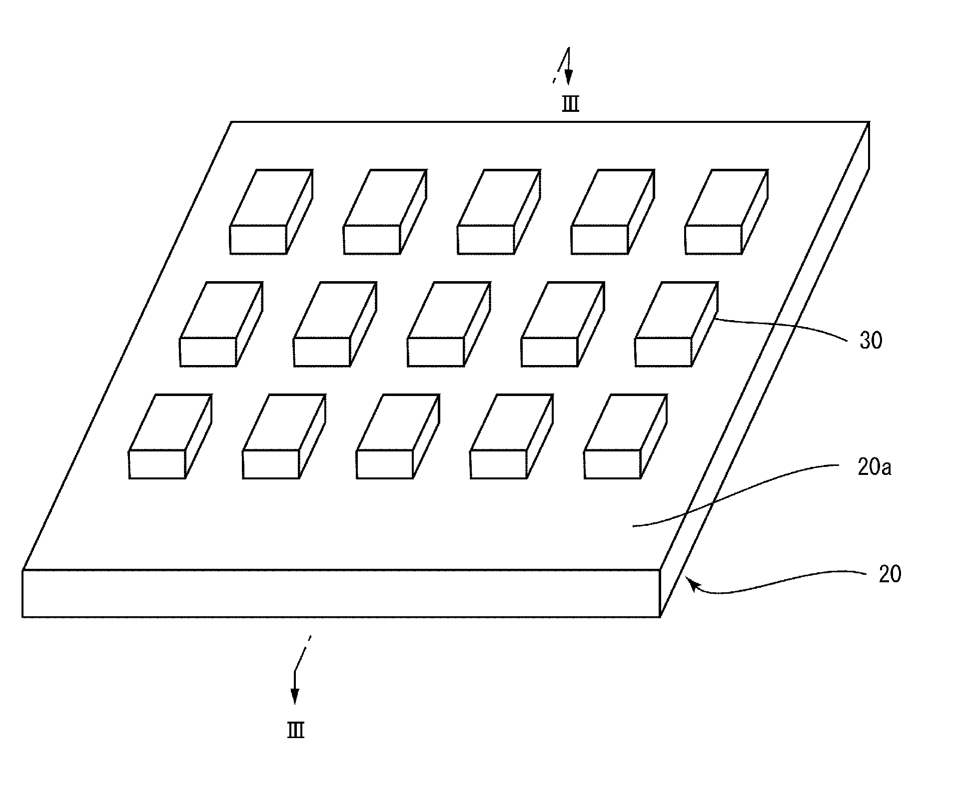
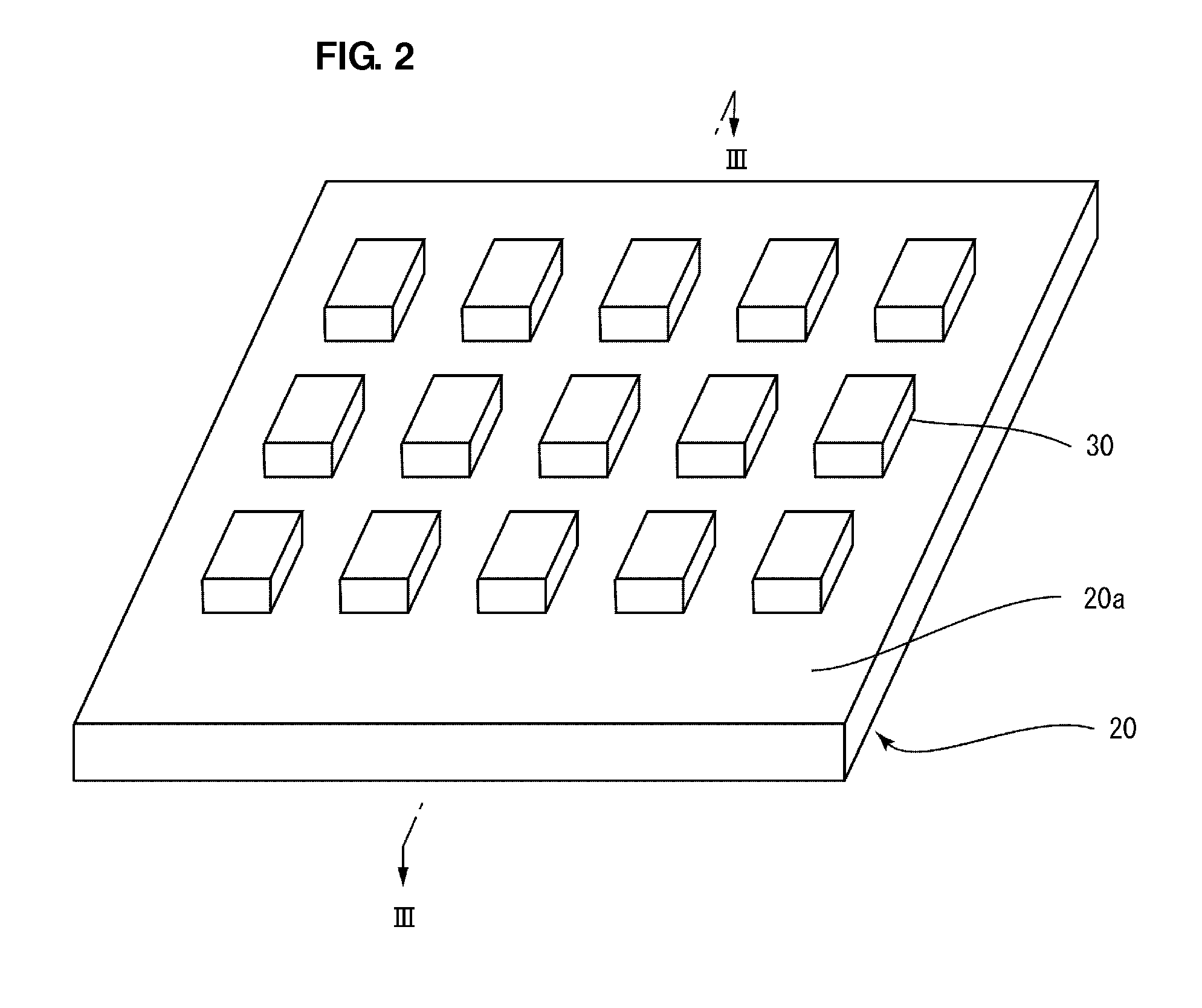
[0040]First, a ceramic electronic component 1 to be produced in the present preferred embodiment will be described with reference to FIGS. 11 to 13.

[0041]For example, the ceramic electronic component 1 defines a ceramic capacitor device, a ceramic piezoelectric device, thermistor device, or an inductor device. Referring to FIGS. 11 to 13, the ceramic electronic component 1 includes a ceramic body 10 preferably having a substantially rectangular parallelepiped shape. More specifically, the ceramic body 10 preferably has a substantially rectangular parallelepiped shape including chamfered corner and edge portions. The ceramic body 10 includes first and second main surfac...


PUM

PropertyMeasurementUnit
Angleaaaaaaaaaa
Angleaaaaaaaaaa
Shapeaaaaaaaaaa

Abstract

A production method for an electronic chip component includes the steps of forming a first paste layer by applying paste onto a first end surface of an electronic component body with a second end surface being stuck onto a substrate having an adhesive surface and drying the paste, turning the electronic component body 180 degrees so as to stick the first end surface of the electronic component body onto the substrate by sliding a slider relative to the substrate in a state in which the slider is in contact with the first end surface of the electronic component body, forming a second paste layer by applying the paste onto the second end surface of the electronic component body and drying the paste, and firing the first and second paste layers.

Description

BACKGROUND OF THE INVENTION[0001]1. Field of the Invention[0002]The present invention relates to a production method for an electronic chip component, and more particularly, to a production method for an electronic chip component in which a functional member, such as an external electrode, formed of paste, is provided on each end surface of a component body.[0003]2. Description of the Related Art[0004]In recent years, multiple electronic chip components have been used in various electronic devices. A specific example of an electronic chip component is a monolithic ceramic capacitor. In general, a monolithic ceramic capacitor includes a ceramic body having a substantially rectangular parallelepiped shape and incorporating first and second internal electrodes that oppose each other, and first and second external electrodes provided on end surfaces of the ceramic body.[0005]In such a monolithic ceramic capacitor, the first and second external electrodes are formed by applying a conduct...

Claims


Application Information

Patent Timeline
IPC IPC(8): H05K3/30H01G4/12H01G4/252H01G4/30H01G13/00
CPCH01G4/232H01G4/30H01G13/006Y10T156/1092Y10T29/49144Y10T29/4913Y10T29/49117Y10T29/49137Y10T29/49133H01G4/12H01G4/252H01G13/00
Inventor DOOKA, MINORUKUNIMOTO, KAZUNORIOGATA, KATSUNORIYAMADA, NAOHIRO
Owner MURATA MFG CO LTD
Features
  • Generate Ideas
  • Intellectual Property
  • Life Sciences
  • Materials
  • Tech Scout
  • Unparalleled Data Quality
  • Higher Quality Content
  • 60% Fewer Hallucinations
Learn More