

Silica glass crucible for pulling up silicon single crystal and method for manufacturing thereof
a technology of silicon single crystal and crucible, which is applied in the direction of crystal growth process, manufacturing tools, and protective fluids, etc., can solve the problems of easy damage to the polysilicon, easy formation of dents, and easy hotness of the crucible bottom, so as to prevent the generation of void defects and high quality
- Summary
- Abstract
- Description
- Claims
- Application Information
AI Technical Summary
Benefits of technology
Problems solved by technology
Method used
Image

Examples
example 1
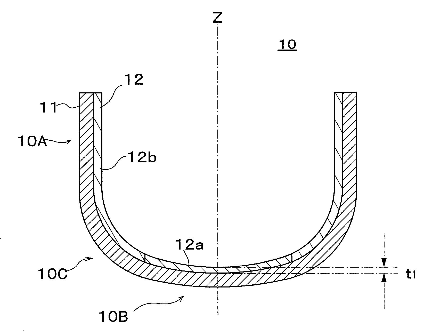
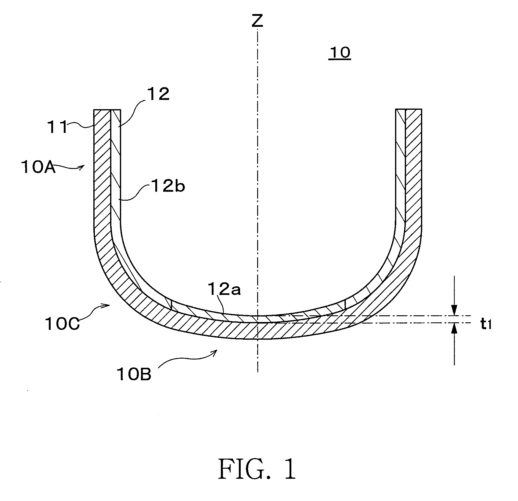
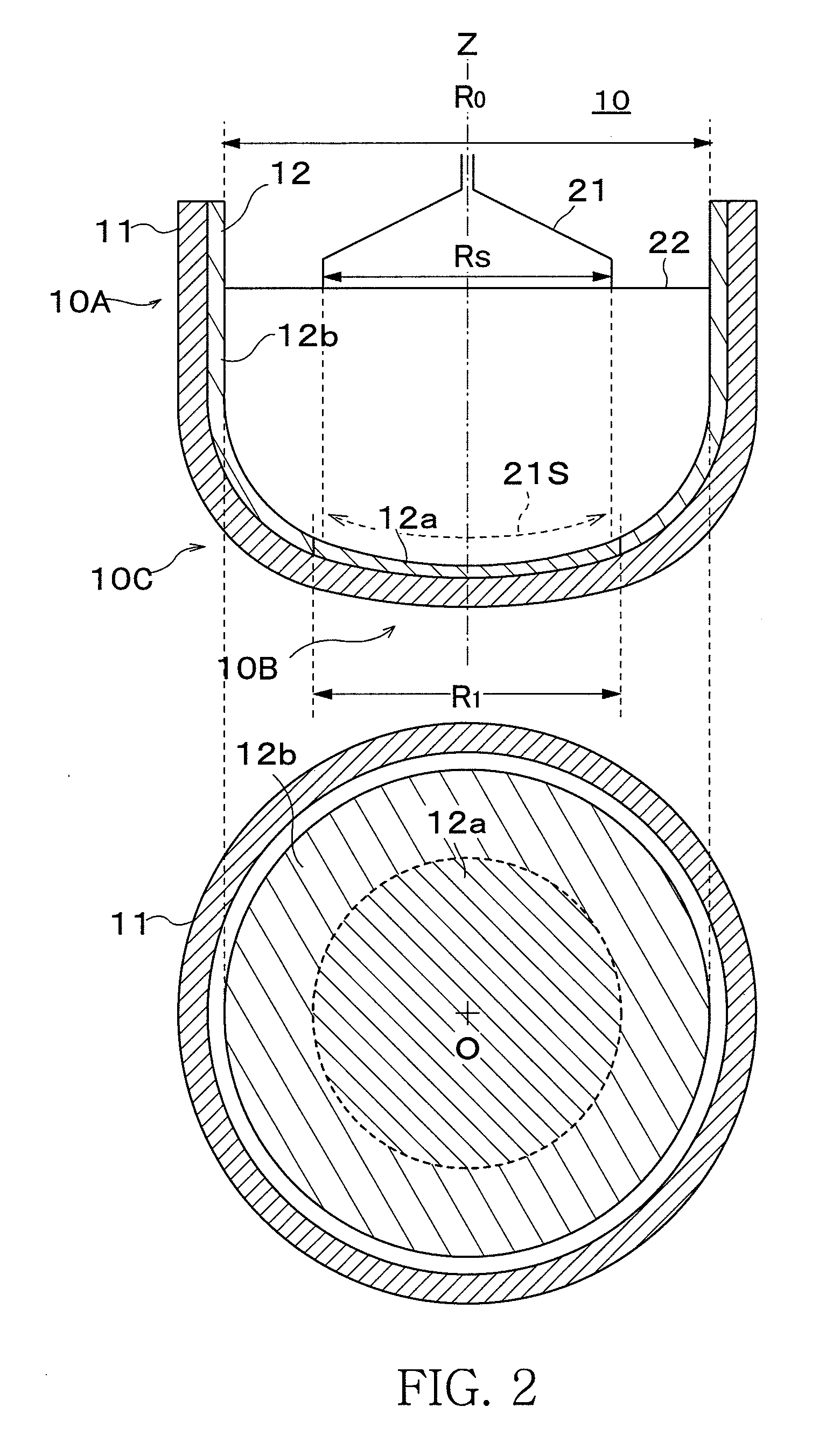
[0053]A sample of a silica glass crucible having the structure shown in FIG. 1 was prepared. The crucible sample had a diameter of 32 inches (diameter R0=800 mm), crucible height of 500 mm, and sidewall section thickness of 17 mm, corner section thickness of 25 mm and bottom section thickness of 14 mm from the inner surface to the exterior surface of the crucible. In addition, the diameter of the first synthetic silica glass layer is 400 mm, thickness was 1.0-1.3 mm (1.0 mm is the thinnest section in the center of the crucible bottom section, 1.3 mm is the thickest section in a periphery position R / 2 from the bottom section center, the same is true below), the average OH group concentration (below referred to simply as OH group concentration) of a range up to a depth of 2 mm from the inner surface of the synthetic silica glass layer was 100 ppm, and the total impurity concentration of Na, K and Li in the natural silica glass layer was 0.5 ppm and the impurity concentration of Al in ...
example 2
[0057]Other than a thickness of the first synthetic silica glass layer being 0.8-1.1 mm and the OH group concentration being 70 ppm, a crucible sample having the same structure as in example 1 was prepared, the silicon single crystal was pulled up under the same conditions as example 1, and the pinhole generation rate of the silicon single crystal ingot was measured. As a result, as shown in Chart 1, the first synthetic silica glass layer was thinner than in example 1, and the pinhole generation rate of example 2 which had a lower OH group concentration was 0.04% which was even lower than the pinhole generation rate of example 1. In addition, the single crystal yield was 1.
example 3
[0058]Other than the total impurity concentration of Na, K and Li of the natural silica glass layer being 0.1%, a crucible sample having the same structure as in example 2 was prepared, the silicon single crystal was pulled up under the same conditions as example 1, and the pinhole generation rate of the silicon single crystal ingot was measured. As a result, as shown in Chart 1, the pinhole generation rate of example 3 which had a lower total impurity concentration of Na, K and Li than example 2 was 0.02%, which was the lowest pinhole generation rate of all the examples. In addition, the single crystal yield was 1.
PUM
| Property | Measurement | Unit |
|---|---|---|
| Length | aaaaa | aaaaa |
| Length | aaaaa | aaaaa |
| Fraction | aaaaa | aaaaa |
Abstract
Description
Claims
Application Information