Multiple-Substrate Transfer Apparatus and Multiple-Substrate Processing Apparatus

a technology of transfer apparatus and substrate, which is applied in the direction of water supply installation, machine/engine, drawing-off water installation, etc., can solve the problems of limiting the wafer transfer rate, increasing the time, and difficulty in charging wafers in-process into the load lock chamber during continuous processing, so as to reduce the cost per throughput and reduce the footprint , the effect of reducing the cost of throughpu

Inactive Publication Date: 2010-06-17
ASM JAPAN +1
View PDF35 Cites 225 Cited by
  • Summary
  • Abstract
  • Description
  • Claims
  • Application Information

AI Technical Summary

Benefits of technology

[0007]The present invention improves the apparatuses devised earlier by the inventors, where its object in an embodiment is to provide ...

Problems solved by technology

With these apparatuses, however, it is difficult to charge wafers in-process into the load lock chamber during continuous processing, such as during a continuous CVD deposition process or when an etching process or ashing process is performed.
However, use of double transfer arms increases the volume of the lo...

Method used


Image

  • Multiple-Substrate Transfer Apparatus and Multiple-Substrate Processing Apparatus
  • Multiple-Substrate Transfer Apparatus and Multiple-Substrate Processing Apparatus
  • Multiple-Substrate Transfer Apparatus and Multiple-Substrate Processing Apparatus

Examples


Embodiment Construction

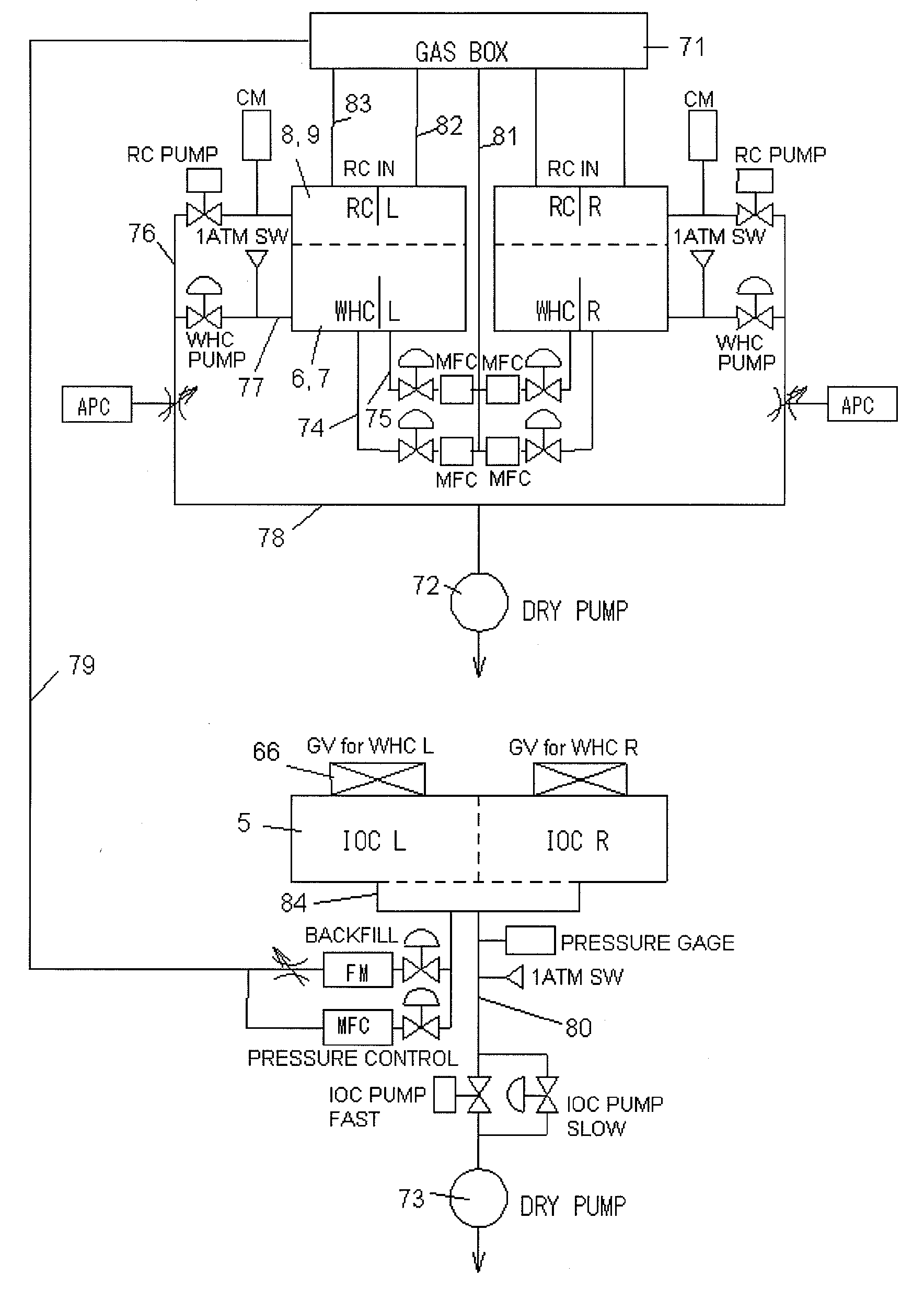
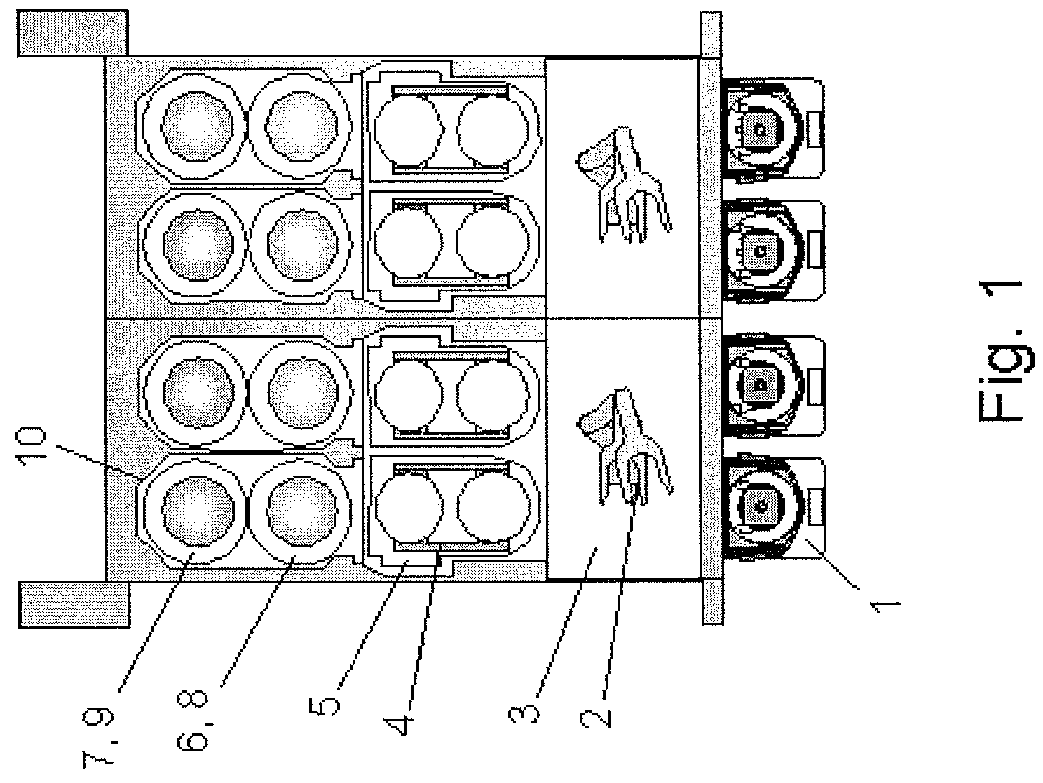
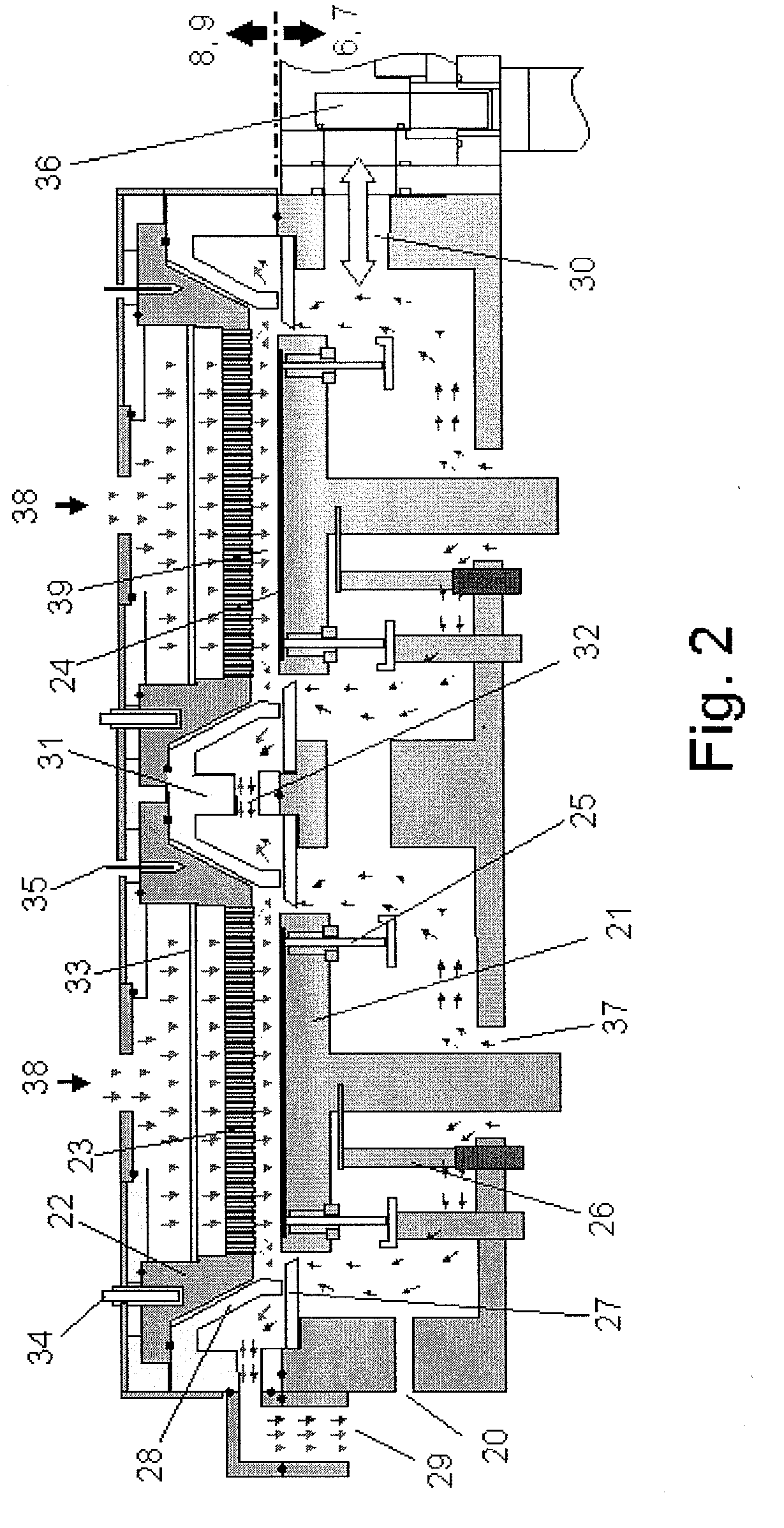
[0021]As described above, embodiments of the present invention, which can resolve at least one of the problems in the conventional apparatuses, include a multiple-substrate processing apparatus comprising: (a) a reaction chamber comprised of two discrete reaction stations for simultaneously processing two substrates, said reaction stations being aligned one behind the other as viewed in a substrate-loading / unloading direction; (b) a transfer chamber disposed underneath the reaction chamber, for loading and unloading substrates to and from the reaction stations simultaneously; (c) a load lock chamber disposed next to the transfer chamber, said load lock chamber being provided with a transfer arm for loading and unloading substrates to and from the transfer chamber, said transfer arm comprising one or more end-effectors for simultaneously supporting two substrates one behind the other as viewed in the substrate-loading / unloading direction; and (d) a transfer robot disposed in the vici...


PUM


Abstract

A multiple-substrate processing apparatus includes: a reaction chamber comprised of two discrete reaction stations aligned one behind the other for simultaneously processing two substrates; a transfer chamber disposed underneath the reaction chamber, for loading and unloading substrates to and from the reaction stations simultaneously; and a load lock chamber disposed next to the transfer chamber. The transfer arm includes one or more end-effectors for simultaneously supporting two substrates one behind the other as viewed in the substrate-loading/unloading direction.

Description

BACKGROUND[0001]1. Field of the Invention[0002]The present invention relates to a semiconductor manufacturing apparatus of vacuum load-lock type, or specifically to the structure and operating method of a compact sheet-feed semiconductor apparatus capable of processing wafers efficiently and continuously or simultaneously, as well as of the gas line system and reactor unit of such apparatus.[0003]2. Description of the Related Art[0004]In general, the chambers of a conventional semiconductor apparatus of vacuum load-lock type used in the manufacture of semiconductor integrated circuits comprise a load lock chamber, a transfer chamber, and multiple reaction chambers (processing chambers) connected to the transfer chamber. In each chamber a wafer transfer robot that automatically supplies wafers is used and operates as follows. First, an atmospheric robot transfers a wafer from a wafer cassette or FOUP (a box equipped with removable wafer cassettes and a front-opening interface) into t...

Claims


Application Information

Patent Timeline
IPC IPC(8): B08B9/00C23C16/54H01L21/306
CPCC23C16/54H01L21/6719H01L21/67754H01L21/67742H01L21/67196Y10T137/0402
Inventor YAMAGISHI, TAKAYUKIKOBAYASHI, TAMIHIRO
Owner ASM JAPAN
Why Eureka
Try Eureka