Light receiving circuit

a light receiving circuit and light technology, applied in the field of light receiving circuits, can solve the problems of light receiving circuit b>2/b> to malfunction, increase in circuit size, and light receiving circuit has a hysteresis characteristic, so as to prevent output signal characteristics, increase circuit size, and hysteresis characteristic

Inactive Publication Date: 2010-06-17
RENESAS ELECTRONICS CORP
View PDF1 Cites 2 Cited by
  • Summary
  • Abstract
  • Description
  • Claims
  • Application Information

AI Technical Summary

Benefits of technology

[0022]In the light receiving circuit according to the first exemplary aspect of the present invention, the bias current control circuit is capable of changing the sensitivity of the light receiving circuit according to the output of the second amplifier. Meanwhile, the second amplifier changes the phase of the output signal of the second amplifier itself according to a photocurrent signal. As a result, the light receiving circuit has a hysteresis characteristic for providing different sensitivities between the rising edge and the falling edge of the photocurrent signal. Consequently, even when the photocurrent signal contains minute current changes, i.e., noise components, output signal characteristics are prevented from being affected by the noise.
[0023]The light receiving circuit according to an exemplary aspect of the present invention prevents occurrence of a malfunction while suppressing an increase in circuit size.

Problems solved by technology

This causes a problem that the noise in the photocurrent Ipd may cause the light receiving circuit 2 to malfunction.
In this case, however, a circuit for imparting the hysteresis characteristic is realized using a differential amplifier circuit or the like in many cases, which results in a problem of an increase in circuit size.
As a result, the light receiving circuit has a hysteresis characteristic for providing different sensitivities between the rising edge and the falling edge of the photocurrent signal.

Method used


Image

  • Light receiving circuit
  • Light receiving circuit
  • Light receiving circuit

Examples


Embodiment Construction

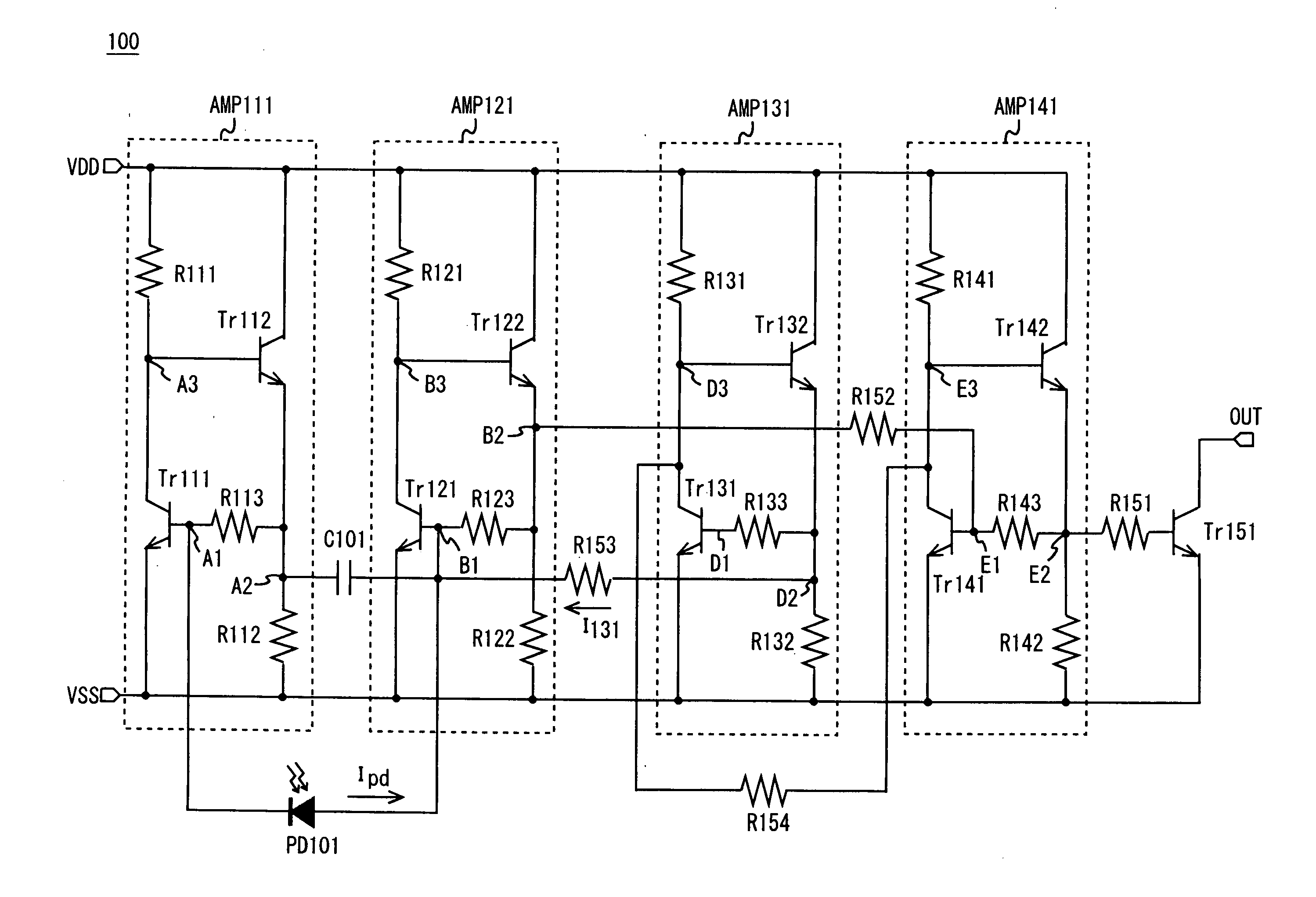
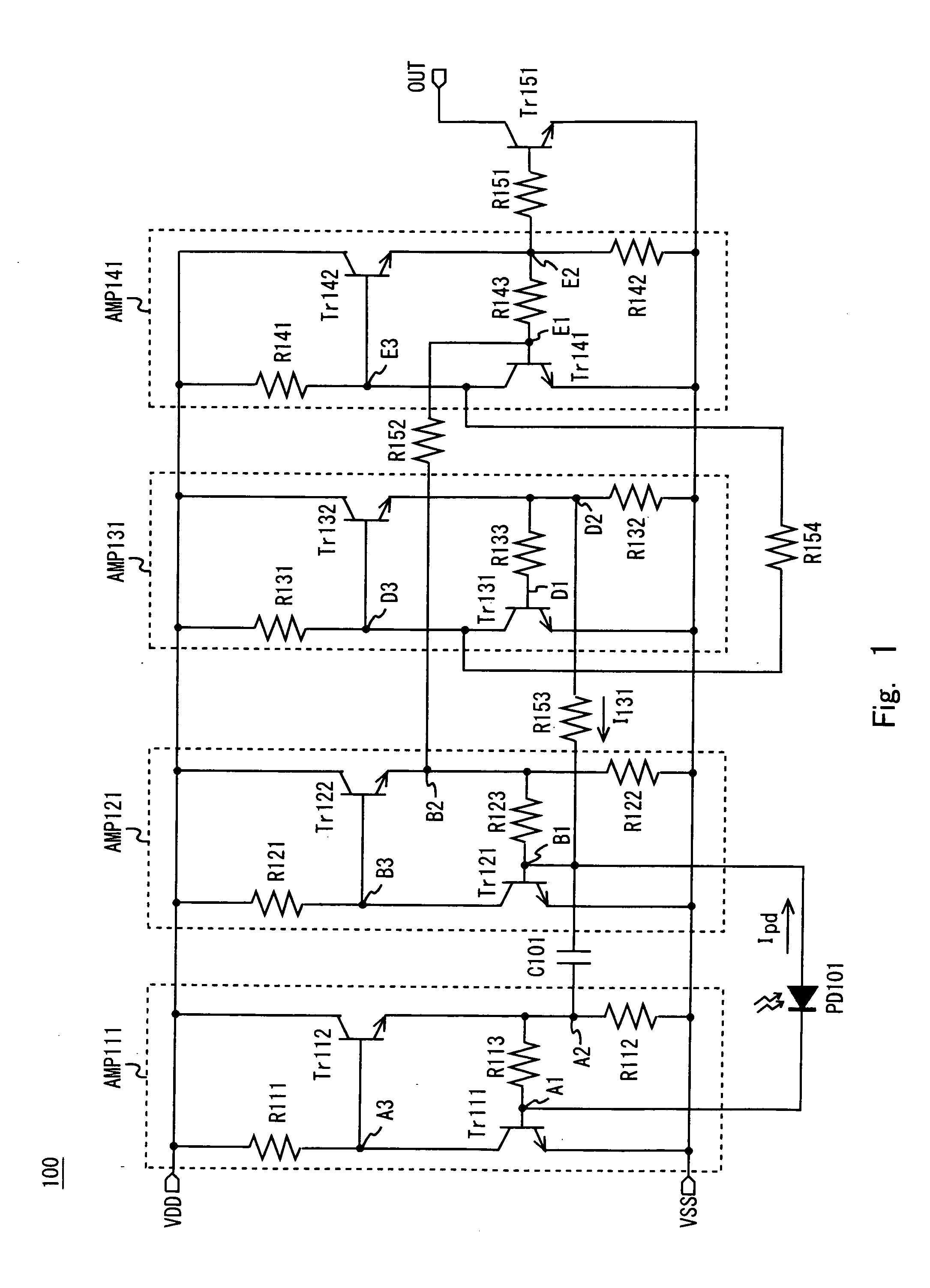
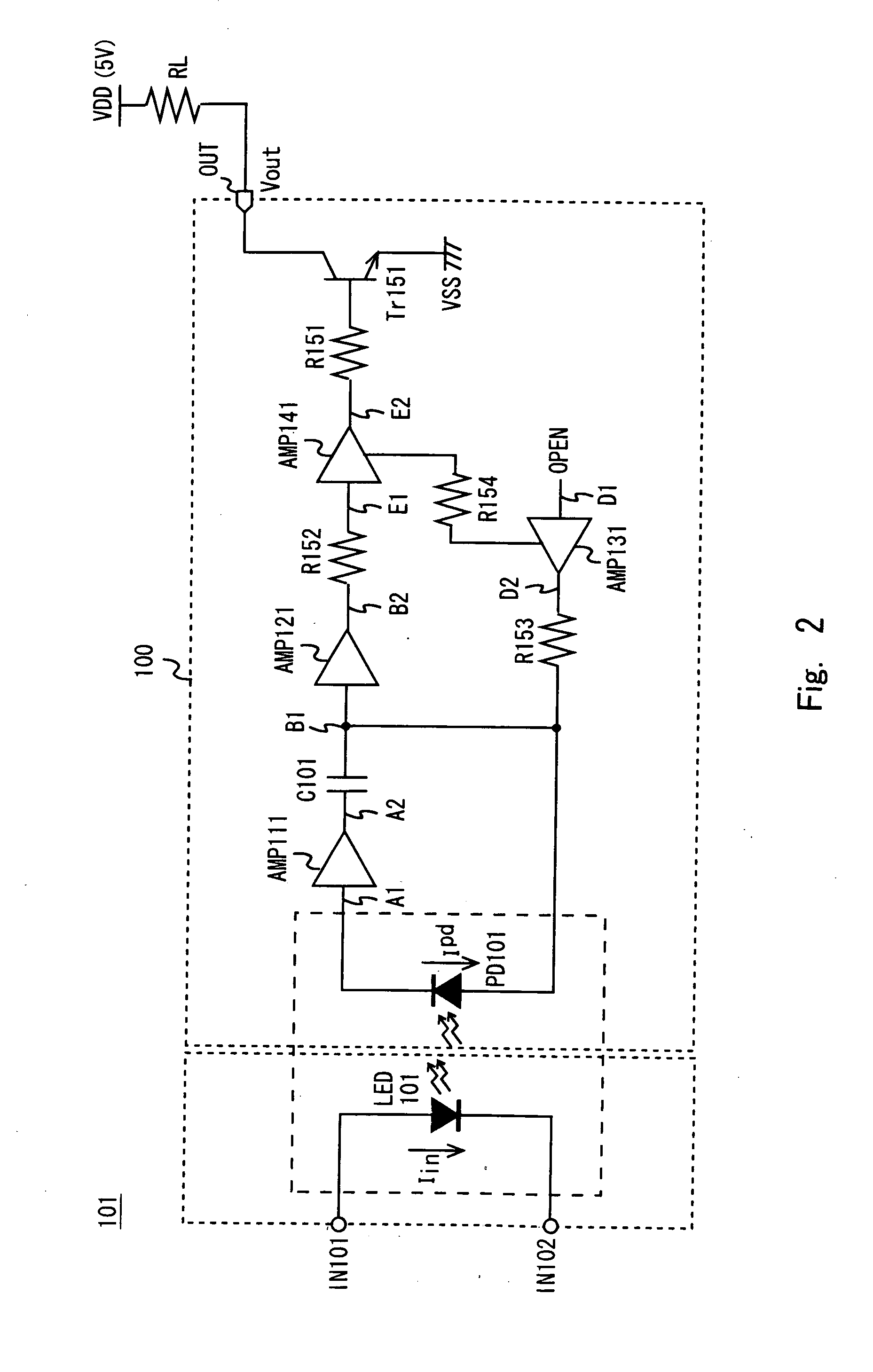
[0035]Exemplary embodiments of the present invention will be described in detail below with reference to the accompanying drawings. In this exemplary embodiment, the present invention is applied to a light receiving circuit of a photocoupler. FIG. 1 shows an exemplary configuration of a light receiving circuit 100 according to this exemplary embodiment.

[0036]As shown in FIG. 1, the light receiving circuit 100 includes amplifiers AMP111, AMP121, AMP131, and AMP141, a photodiode PD101, a capacitor element C101, an NPN transistor Tr151, and resistor elements R151 to R153.

[0037]The amplifier AMP111 includes NPN transistors Tr111 and Tr112 and resistor elements R111 to R113. The NPN transistor Tr111 has a collector connected to a node A3, an emitter connected to a ground voltage terminal VSS, and a base connected to a node A1. The NPN transistor Tr112 has a collector connected to a power supply voltage terminal VDD, an emitter connected to a node A2, and a base connected to the node A3. ...


PUM


Abstract

Provided is a light receiving circuit including: a photodiode; a first amplifier including a feedback resistor connected between an input and an output of an inverting amplifier and having an input connected to a cathode of the photodiode; a second amplifier having a configuration similar to that of the first amplifier and having an input connected to an anode of the photodiode; a capacitor element connected between an output of the first amplifier and the input of the second amplifier; and a bias current control circuit that outputs a bias current to the input of the second amplifier according to a current value of the photocurrent, and controls an output voltage signal of the light receiving circuit according to an output of the second amplifier by using the bias current to adjust the sensitivity. The bias current control circuit changes the sensitivity according to the output of the second amplifier.

Description

BACKGROUND[0001]1. Field of the Invention[0002]The present invention relates to a light receiving circuit.[0003]2. Description of Related Art[0004]At present, photocouplers are widely used. Each photocoupler is used in a device including a drive unit operating at high voltage for industrial and consumer use in order to ensure electrical isolation between the drive unit operating at high voltage and a control unit operating at low voltage. The photocoupler transmits an electrical input signal to an output side by turning on / off light, and outputs the light as an electrical signal again.[0005]A general-purpose photocoupler is required to be low in price and high in reliability. A circuit configuration in which such a photocoupler can be used as a light receiving circuit is disclosed in Japanese Unexamined Patent Application Publication No. 2004-328061. FIG. 5 shows a circuit diagram of a light receiving circuit 1 of a prior art disclosed in Japanese Unexamined Patent Application Publi...

Claims


Application Information

Patent Timeline
Patent Type & Authority Applications(United States)
IPC IPC(8): H03F3/10
CPCH03F3/08
Inventor OKU, SETSUYA
Owner RENESAS ELECTRONICS CORP
Why Eureka
Try Eureka