Ferroelectric thin film, method of manufacturing the same, ferroelectric memory device and ferroelectric piezoelectric device

a technology of ferroelectric memory and ferroelectric piezoelectric device, which is applied in the direction of basic electric elements, semiconductor devices, electrical apparatus, etc., can solve the problems of not being able to secure the b>10/b>-year guarantee generally required for semiconductors, and not being put into commercial use as ferroelectric memory devices

Inactive Publication Date: 2005-04-07
SEIKO EPSON CORP
View PDF4 Cites 4 Cited by
  • Summary
  • Abstract
  • Description
  • Claims
  • Application Information

AI Technical Summary

Problems solved by technology

Since the 1T ferroelectric memory device has retention time (data retention time) as short as one month due to occurrence of an internal electric field in the capacitor because of its structure, it is considered to be impossible to secure a 10-year guarantee generally required for semiconductors.
However, PZT in the tetragonal region has not been put into commercial use as a ferroelectric memory device since reliability cannot be secured.
Moreover, Pb has the smallest bond energy with oxygen (38.8 kcal / mol), and tends to cause Pb deficiency to occur in the PZT crystal.
These defects result in space charge polarization, and cause imprint characteristics to deteriorate.
Moreover, O deficiency occurs from the charge neutrality principle, whereby Schottky defects occur due to the ionic crystal structure.
This causes leakage current characteristics to deteriorate, whereby reliability cannot be secured.
Therefore, in the case of using PZT as the ferroelectric material, it is impossible to utilize the Zr-rich composition used for a small capacity memory.
However, if the hysteresis shape becomes further narrowed, deterioration of imprint characteristics will come to the surface.
This causes the above-described problems to occur.
Therefore, it is impossible to increase the integration of the ferroelectric memory unless the problems of Ti-rich PZT are solved.
However, this technology does not describe the hysteresis loop of the ferroelectric capacitor necessary for the operation in detail.
Specifically, it becomes difficult to use the ferroelectric capacitor at a low voltage.

Method used


Image

  • Ferroelectric thin film, method of manufacturing the same, ferroelectric memory device and ferroelectric piezoelectric device
  • Ferroelectric thin film, method of manufacturing the same, ferroelectric memory device and ferroelectric piezoelectric device
  • Ferroelectric thin film, method of manufacturing the same, ferroelectric memory device and ferroelectric piezoelectric device

Examples


example 1

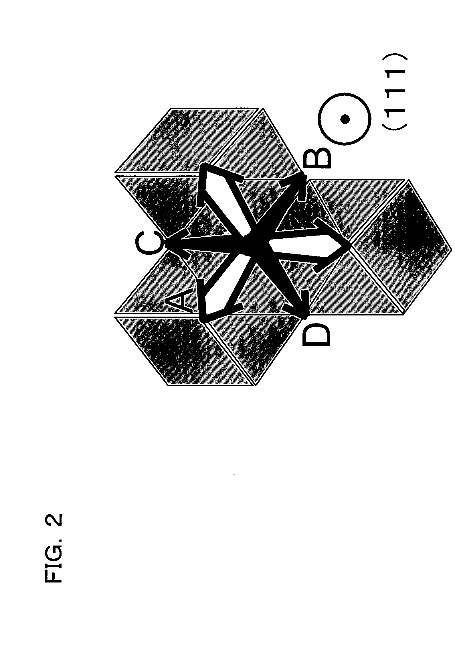
[0053]FIG. 3 shows an orientation plane suitable for device applications determined for PZT having a tetragonal structure. In FIG. 3, bulk values are used as the lattice constant, polarization axis direction (90° domain necessarily exists with the 180° domain), and polarization. The state in which the polarization axes infinitely exist in a rotated state in the film plane is shown by using six directions for convenience of illustration. As candidates for the orientation planes, orientation planes with high existence probability selected from JCPDS were used. In FIG. 3, the multiplicity means the degree in which the polarization axes completely overlap when determining the orientation plane suitable for device applications using the above parameters. In the case where two or more polarization axes remain, the higher the multiplicity, the higher the existence probability. The polarization axis with higher multiplicity effectively contributes to polarization with higher probability.

[0...

example 2

[0060] In this example, a PbZr0.4Ti0.6O3 ferroelectric thin film was formed.

[0061] A conventional method uses a solution containing Pb in an excess amount of about 20%. This aims at preventing volatilization of Pb and reducing the crystallization temperature. However, since the state of the excess Pb in the resulting thin film is unknown, the amount of excess Pb should be limited to the minimum.

[0062] A PbZr0.4Ti0.6O3 thin film with a thickness of 200 nm was formed according to a flow shown in FIG. 8 by using 10 wt % sol-gel solutions for forming PbZr0.4Ti0.6O3 (solvent: n-butanol) in which the amount of excess Pb was 0%, 5%, 10%, 15%, and 20%, and further adding 1 mol % of a 10 wt % sol-gel solution for forming PbSiO3 (solvent: n-butanol). FIG. 9 shows XRD patterns and surface morphology of the resulting thin films.

[0063] About 20% excess Pb is necessary in a conventional method. However, it was found that crystallization sufficiently proceeds with the addition of 5% excess Pb. ...


PUM


Abstract

A ferroelectric thin film formed of a highly oriented polycrystal in which 180° domains and 90° domains arrange at a constant angle to an applied electric field direction in a thin film plane and reversely rotate in a predetermined electric field.

Description

[0001] Japanese Patent Application No. 2002-379418, filed on Dec. 27, 2002, is hereby incorporated by reference in its entirety. BACKGROUND OF THE INVENTION [0002] In recent years, research and development of a thin film such as PZT or SBT, and a ferroelectric capacitor and a ferroelectric memory device using such a thin film have been extensively conducted. The structure of the ferroelectric memory device is roughly divided into 1T, 1T1C, 2T2C, and simple matrix. Since the 1T ferroelectric memory device has retention time (data retention time) as short as one month due to occurrence of an internal electric field in the capacitor because of its structure, it is considered to be impossible to secure a 10-year guarantee generally required for semiconductors. The 1T1C and 2T2C ferroelectric memory devices have almost the same configuration as that of a DRAM, and include a select transistor. Therefore, the DRAM manufacturing technology can be utilized. Moreover, since the 1T1C and 2T2C ...

Claims


Application Information

Patent Timeline
Patent Type & Authority Applications(United States)
IPC IPC(8): H01L21/316H01L21/8246H01L27/105
CPCH01L21/31691H01L21/02197H01L21/02282H01L21/02356H01L21/02337
Inventor KIJIMA, TAKESHIHAMADA, YASUAKINATORI, EIJI
Owner SEIKO EPSON CORP
Why Eureka
Try Eureka