Densification process for titanium nitride layer for submicron applications

a technology of titanium nitride and densification process, which is applied in the direction of coating, chemical vapor deposition coating, metallic material coating process, etc., can solve the problems of voids formed in the via or trench, the deposition process has difficulty filling the submicron structure, and the amount of ongoing effort is directed

Inactive Publication Date: 2010-06-17
APPLIED MATERIALS INC
View PDF45 Cites 44 Cited by
  • Summary
  • Abstract
  • Description
  • Claims
  • Application Information

AI Technical Summary

Benefits of technology

[0012]Embodiments of the present invention provide methods of forming and densifying a titanium nitride barrier layer. In one embodiment, a method for forming a titanium nitride barrier layer on a substrate includes depositing a titanium nitride layer on the substrate by a metal-organic chemical vapor deposition process, and performing a plasma treatment process on the deposited titanium nitride layer, wherein the plasma treatment process operates to densify the deposited titanium nitride layer, resulting in a densified titanium nitride layer, wherein the plasma treatment process further comprises supplying a plasma gas mixture containing a nitrogen gas to hydrogen gas ratio between about 20:1 and about 3:1, and applying less than about 500 Watts RF power to the plasma gas mixture.
[0013]In another embodiment, a method for forming a titanium nitride barrier layer on a substrate includes depositing a first titanium nitride layer to a thickness of between about 10 Å and about 20 Å by a first metal-organic chemical vapor deposition process, plasma treating the first titanium nitride layer by applying less than about 500 Watts RF power to a plasma gas mixture comprising n

Problems solved by technology

However, as the fringes of circuit technology are pressed, the shrinking dimensions of interconnects in VLSI and ULSI technology have placed additional demands on the processing capabilities.
Many traditional deposition processes have difficulty filling submicron structures where the aspect ratio exceeds 4:1.
Therefore, there is a great amount of ongoing effort being directed at the formation of substantially void-free and seam-free and conformal submicron features having high aspect ratios.
A variety of problems that eventually may lead to device failure may result from the specific process used to deposit or form the titanium nitride layer.
For example, titanium nitride barrier layers deposited using a PVD process often suffer from poor step coverage, overhang, and voids formed within the via or trench when the via is less than 50 nm or having an aspect ratio greater than 4:1.
Insufficient deposition on the bottom and sidewall of the vias or trenches can also result in deposition discontinuity, thereby resulting in device shorting or poor interconnection formation.
Furthermore, the titanium nitride

Method used


Image

  • Densification process for titanium nitride layer for submicron applications
  • Densification process for titanium nitride layer for submicron applications
  • Densification process for titanium nitride layer for submicron applications

Examples


Embodiment Construction

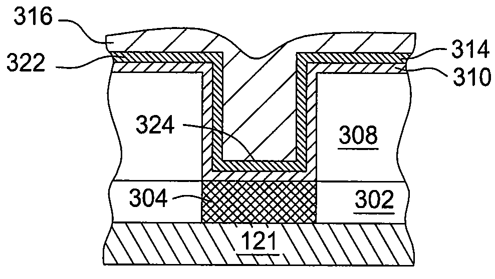
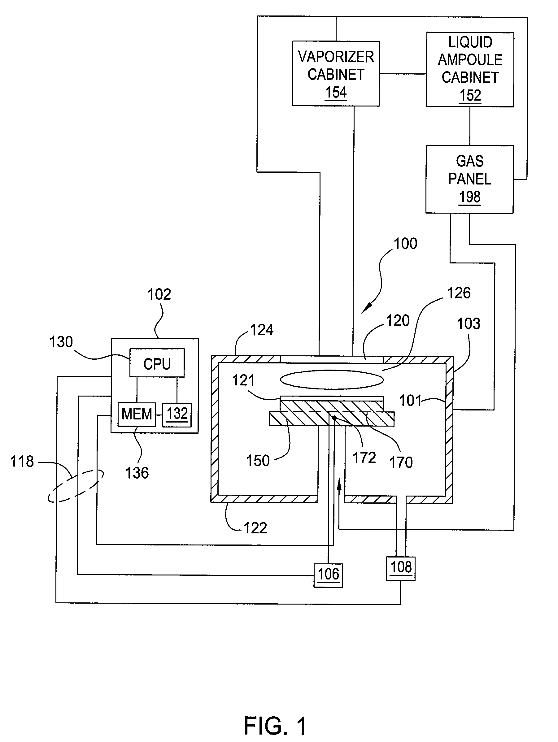
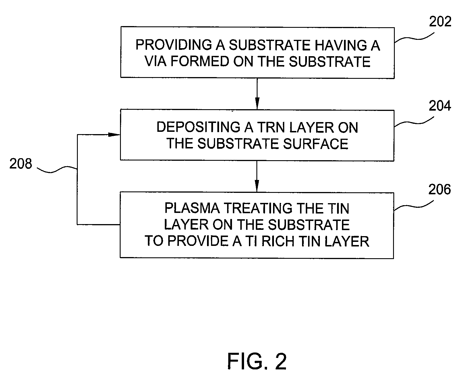
[0019]One embodiment of the invention provides a method of forming and densifying a titanium nitride layer on a substrate by exposing the substrate to a hydrogen and nitrogen containing light plasma. The densification process is performed at a relatively low RF plasma power and a high nitrogen to hydrogen ratio so as to provide a substantially titanium rich titanium nitride barrier layer. The titanium nitride barrier material may contain a single densified titanium nitride layer or a titanium nitride barrier stack containing two, three, or more densified titanium nitride layers. Each densified titanium nitride layers may have a thickness of about 20 Å or less. Subsequent to exposing the substrate to a hydrogen or nitrogen containing plasma process, the method provides exposing the substrate to air for a predetermined time period prior to depositing a conductive layer on the substrate. In one embodiment, the titanium nitride layer is deposited by a CVD process, a MOCVD process, an AL...


PUM

PropertyMeasurementUnit
Timeaaaaaaaaaa
Timeaaaaaaaaaa
Timeaaaaaaaaaa

Abstract

Embodiments of the present invention provide methods of forming and densifying a titanium nitride barrier layer. The densification process is performed at a relatively low RF plasma power and high nitrogen to hydrogen ratio so as to provide a substantially titanium rich titanium nitride barrier layer. In one embodiment, a method for forming a titanium nitride barrier layer on a substrate includes depositing a titanium nitride layer on the substrate by a metal-organic chemical vapor deposition process, and performing a plasma treatment process on the deposited titanium nitride layer, wherein the plasma treatment process operates to densify the deposited titanium nitride layer, resulting in a densified titanium nitride layer, wherein the plasma treatment process further comprises supplying a plasma gas mixture containing a nitrogen gas to hydrogen gas ratio between about 20:1 and about 3:1, and applying less than about 500 Watts RF power to the plasma gas mixture.

Description

BACKGROUND OF THE INVENTION[0001]1. Field of the Invention[0002]Embodiments of the invention generally relate to a fabrication process for forming a barrier layer on a substrate, and more particularly, to a densification process for a titanium nitride barrier material on semiconductor substrates.[0003]2. Description of the Related Art[0004]Reliably producing submicron and smaller features is one of the key technologies for the next generation of very large scale integration (VLSI) and ultra large scale integration (ULSI) of semiconductor devices. However, as the fringes of circuit technology are pressed, the shrinking dimensions of interconnects in VLSI and ULSI technology have placed additional demands on the processing capabilities. The multilevel interconnects that lie at the heart of this technology require precise processing of high aspect ratio features, such as vias and other interconnects. Reliable formation of these interconnects is very important to VLSI and ULSI success a...

Claims


Application Information

Patent Timeline
IPC IPC(8): H01L21/441H01L21/443
CPCC23C16/34C23C16/56H01L21/28556H01L21/76862H01L21/76846H01L21/76856H01L21/76843
Inventor RITCHIE, ALAN ALEXANDERHASSAN, MOHD FADZIL ANWAR
Owner APPLIED MATERIALS INC
Why Eureka
Try Eureka