Thin film transistor using boron-doped oxide semiconductor thin film and method of fabricating the same

a thin film transistor and boron-doped oxide technology, applied in the direction of transistors, semiconductor devices, electrical devices, etc., can solve the problems of device uniformity, irregularity in such devices, and technical restrictions, and achieve the effect of ensuring stability

Active Publication Date: 2010-06-24
ELECTRONICS & TELECOMM RES INST
View PDF5 Cites 75 Cited by
  • Summary
  • Abstract
  • Description
  • Claims
  • Application Information

AI Technical Summary

Benefits of technology

[0022]The present invention is also directed to a method of fabricating a thin film transistor capable of optimizing a f...

Problems solved by technology

While there are non-transparent semiconductors such as CdS, ZnS, ZnSe, etc, as non-ZnO-based materials and their properties can be applied to AMOLED, non-transparent properties cause technical restrictions.
Since an amorphous silicon transistor has a low mobility of about 1 cm/Vs and a polysilicon transistor has a high mobility of about 100 cm/Vs, there may be irregularity in such devices.
In the case of the ZnO-based thin film transistors, characteristics of a thin film may vary sensitively depending on humidity in the air, annealing, and manufacturing processes, which may cause stability problems, and a crystalline channel may cause a problem in dev...

Method used


Image

  • Thin film transistor using boron-doped oxide semiconductor thin film and method of fabricating the same
  • Thin film transistor using boron-doped oxide semiconductor thin film and method of fabricating the same
  • Thin film transistor using boron-doped oxide semiconductor thin film and method of fabricating the same

Examples


embodiment 1

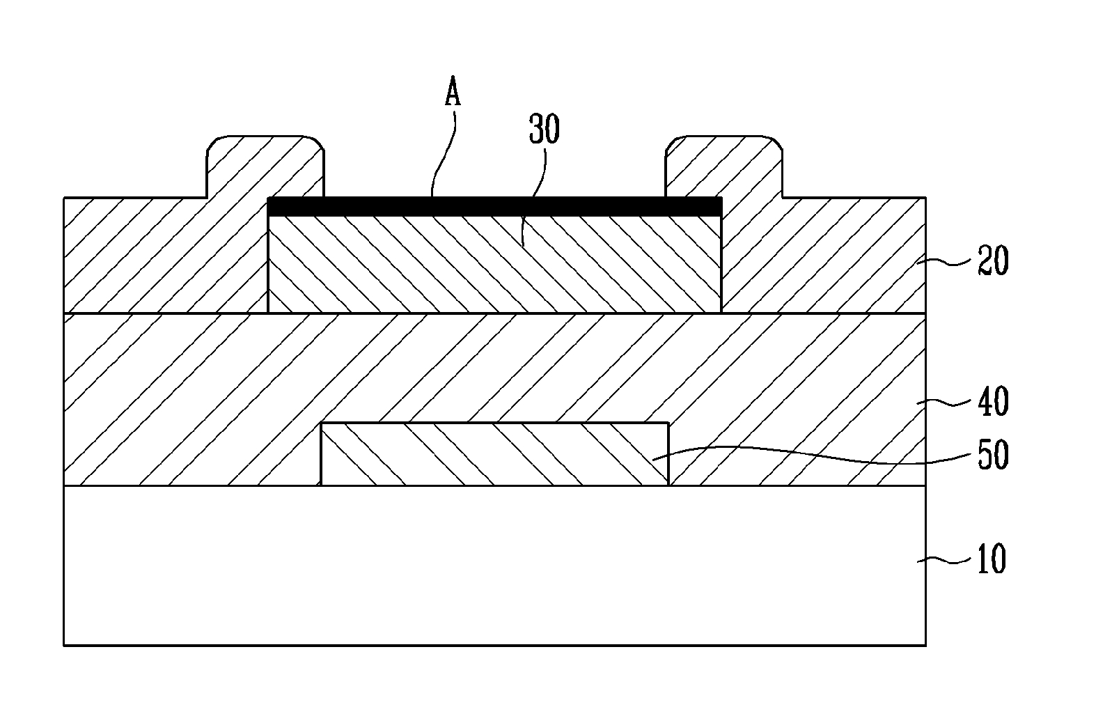
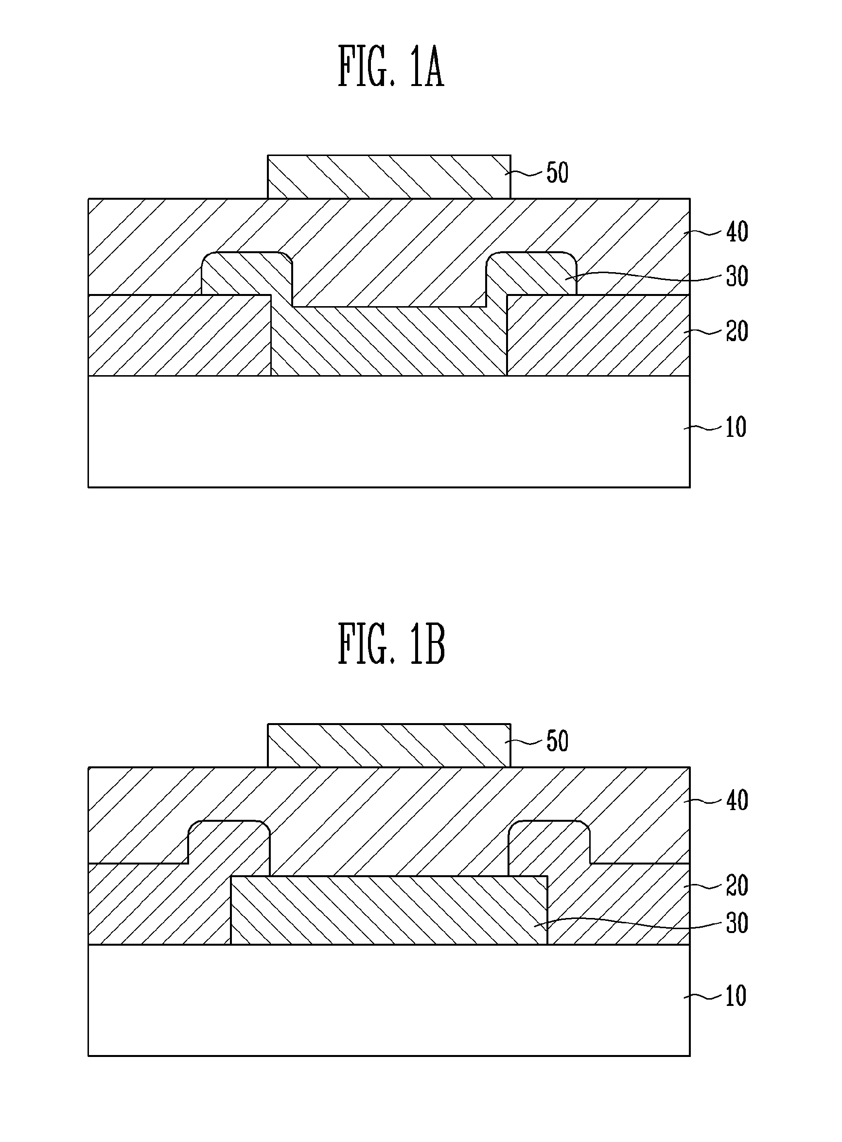
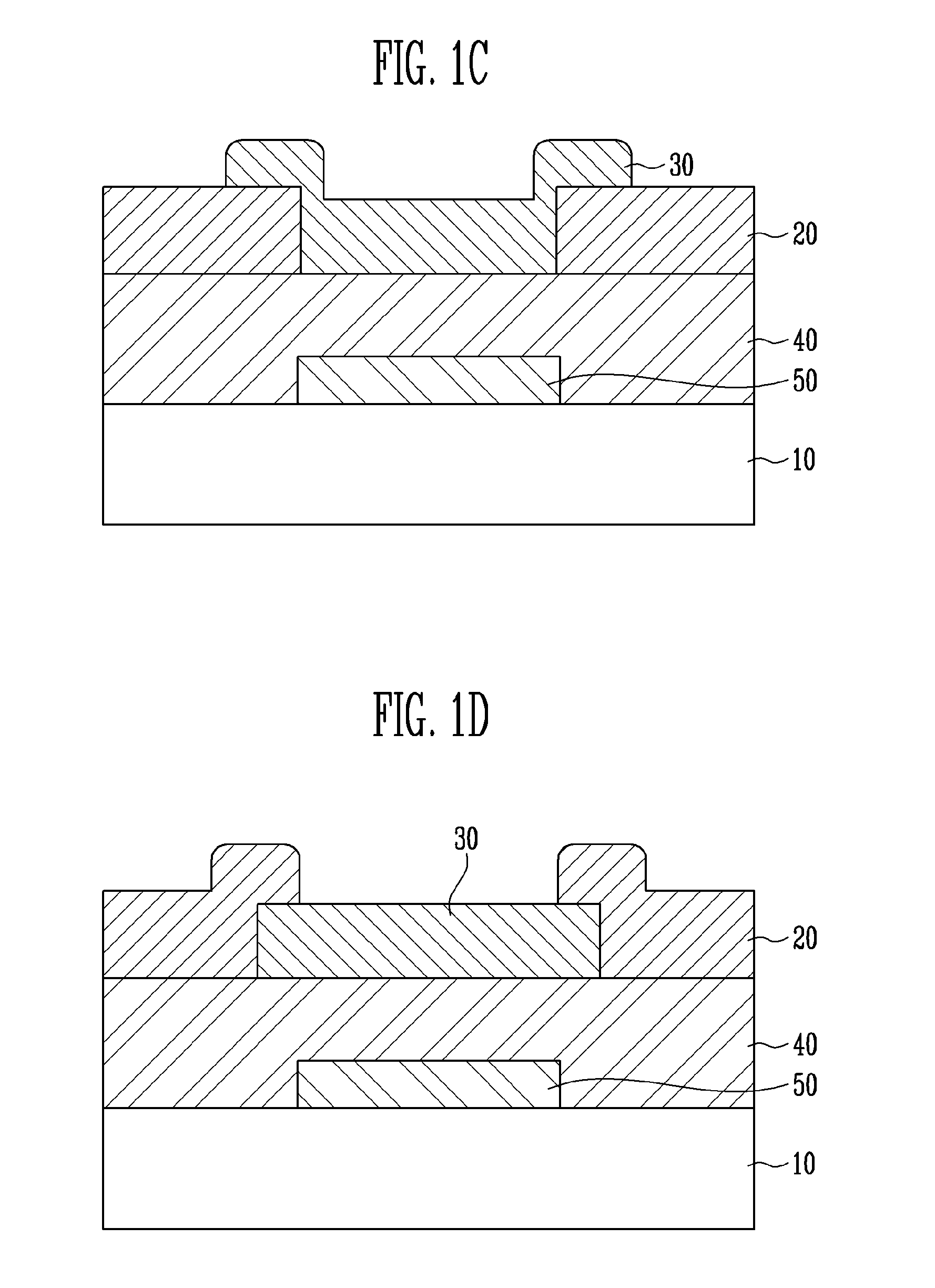
[0064]Source and drain electrodes were deposited on a substrate to a thickness of 150 nm using ITO through sputtering, and then, the source and drain electrodes were etched and patterned using a mixed solution of phosphoric acid and nitric acid at a temperature of 50° C. Next, ZTO (Zn:Sn atomic ratio: 3:1) doped with boron of 3.5 at % was deposited on the source and drain electrodes at a normal temperature through sputtering to form a boron-doped ZTO channel layer to a thickness of 20 nm, and then, annealed at a temperature of 400° C. for one hour. Then, a channel protection layer was formed on the channel layer to a thickness of 10 nm using alumina. Next, the channel layer and the channel protection were wet-etched and patterned using a dilute HF solution. Next, a gate insulating layer was formed on the patterned channel layer and channel protection layer to a thickness of 190 nm using alumina through ALD at a temperature of 150° C., and then, the gate insulating layer was etched u...

embodiment 2

[0067]Source and drain electrodes were deposited on a substrate to a thickness of 150 nm using ITO through sputtering, and then, etched and patterned using a mixed solution of phosphoric acid and nitric acid at a temperature of 50° C. Next, a boron-doped ZITO channel layer was formed on the source and drain electrodes at a normal temperature through sputtering to a thickness of 20 nm using ZITO (Zn:In:Sn atomic ratio: 3:2:1) doped with boron of 3.5 at %, and then, annealed at a temperature of 200° C. for one hour. Next, a channel protection layer was formed on the channel layer to a thickness of 10 nm using alumina. Next, the channel layer and the channel protection layer were wet-etched and patterned using a dilute HF solution. Then, a gate insulating layer was formed on the patterned channel layer and channel protection layer using alumina to a thickness of 190 nm at a temperature of 150° C. through ALD, and then, the gate insulating layer was etched and patterned using a phosphor...

embodiment 3

[0068]A thin film transistor was fabricated in the same manner as in Embodiment 2, except that annealing was performed at a temperature of 300° C. for one hour upon formation of a channel layer. Characteristics of the fabricated transistor were estimated and the results are shown in FIG. 6. As can be appreciated from FIG. 6, an SS value was 0.29 and mobility was 13.96 cm2 / sV.


PUM


Abstract

Provided are a thin film transistor, to which a boron-doped oxide semiconductor thin film is applied as a channel layer, and a method of fabricating the same. The thin film transistor includes source and drain electrodes, a channel layer, a gate insulating layer, and a gate electrode, which are formed on a substrate. The channel layer is an oxide semiconductor thin film doped with boron. Therefore, it is possible to remarkably improve electrical characteristics and high temperature stability of the thin film transistor.

Description

CROSS-REFERENCE TO RELATED APPLICATION[0001]This application claims the benefit of Korean Patent Application No. 10-2008-0129691, filed Dec. 18, 2008, the disclosure of which is hereby incorporated herein by reference in its entirety.BACKGROUND[0002]1. Field of the Invention[0003]The present invention relates to a thin film transistor using a boron-doped oxide semiconductor thin film and a method of fabricating the same, and more particularly, to a thin film transistor using a boron-doped oxide semiconductor thin film as a channel layer to remarkably improve electrical characteristics and a method of fabricating the same.[0004]2. Discussion of Related Art[0005]In manufacturing thin film transistors, a ZnO-based material, a non-ZnO-based material and a silicon-based material are mainly used to form a channel layer. These materials will be described in detail.[0006](1) ZnO-Based Material[0007]Methods of adjusting a ratio of zinc and oxygen (Zn / O) when forming a channel layer using ZnO...

Claims


Application Information

Patent Timeline
IPC IPC(8): H01L29/26H01L29/786H01L21/34
CPCH01L21/0237H01L21/02554H01L21/02565H01L29/7869H01L21/02631H01L29/78606H01L21/02573H01L29/06
Inventor CHEONG, WOO SEOKCHUNG, SUNG MOOKRYU, MIN KIHWANG, CHI SUNCHU, HYE YONG
Owner ELECTRONICS & TELECOMM RES INST
Why Eureka
Try Eureka