Method for manufacturing composite substrate and composite substrate

a composite substrate and manufacturing method technology, applied in the direction of piezoelectric/electrostrictive transducers, generators/motors, transducer types, etc., can solve the problems of frequent occurrence of chipping from the edge, and the adhesive layer is not fully applied, so as to reduce the thickness of the piezoelectric substrate

Active Publication Date: 2010-06-24
NGK INSULATORS LTD
View PDF8 Cites 30 Cited by
  • Summary
  • Abstract
  • Description
  • Claims
  • Application Information

AI Technical Summary

Benefits of technology

[0005]Such composite substrates are often manufactured by preparing a piezoelectric substrate and a supporting substrate, bonding the piezoelectric substrate to the supporting substrate with an organic adhesive layer interposed therebetween, and reducing the thickness of the piezoelectric substrate. Since an edge of a substrate may hit something and be broken during handling, a piezoelectric substrate is generally beveled. When the thickness of a piezoelectric substrate is decreased, abrasive grains are placed between a surface of a piezoelectric substrate and a lapping plate, and the surface of the piezoelectric substrate is lapped with the lapping plate. However, according to such a manufacturing method, when a piezoelectric substrate and a supporting substrate are bonded together, an organic adhesive layer is not fully applied up to a beveled edge of the piezoelectric substrate. Furthermore, since beveling increases the distance between the piezoelectric substrate and the supporting substrate, an edge of the piezoelectric substrate is not bonded to the supporting substrate. In such a state, lapping of the surface of the piezoelectric substrate with a lapping plate causes a problem of frequent occurrence of chipping from the edge.
[0011](d) placing abrasive grains between the surface of the piezoelectric substrate and a lapping plate, and lapping the surface of the piezoelectric substrate with the lapping plate to reduce the thickness of the piezoelectric substrate and performing mirror polishing of the surface of the piezoelectric substrate,

Problems solved by technology

However, according to such a manufacturing method, when a piezoelectric substrate and a supporting substrate are bonded together, an organic adhesive layer is not fully applied up to a beveled edge of the piezoelectric substrate.
In such a state, lapping of the surface of the piezoelectric substrate with a lapping plate causes a problem of frequent occurrence of chipping from the edge.

Method used


Image

  • Method for manufacturing composite substrate and composite substrate
  • Method for manufacturing composite substrate and composite substrate
  • Method for manufacturing composite substrate and composite substrate

Examples


example 1

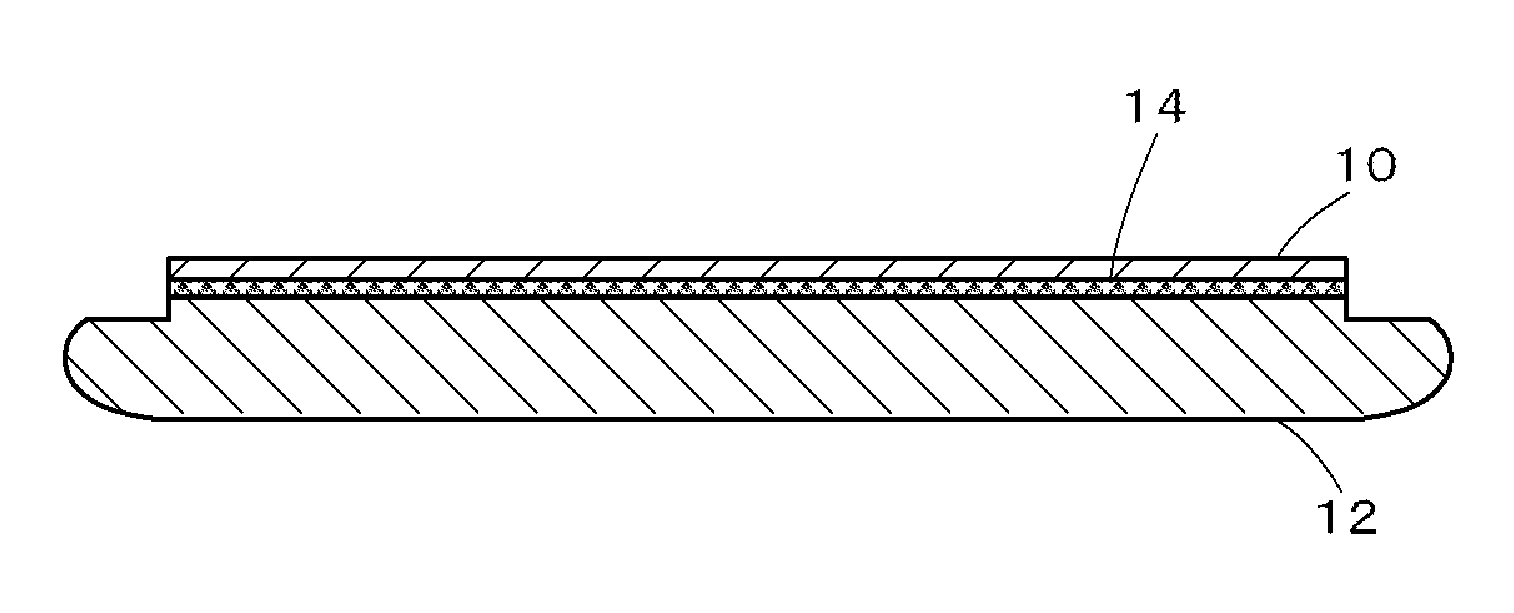
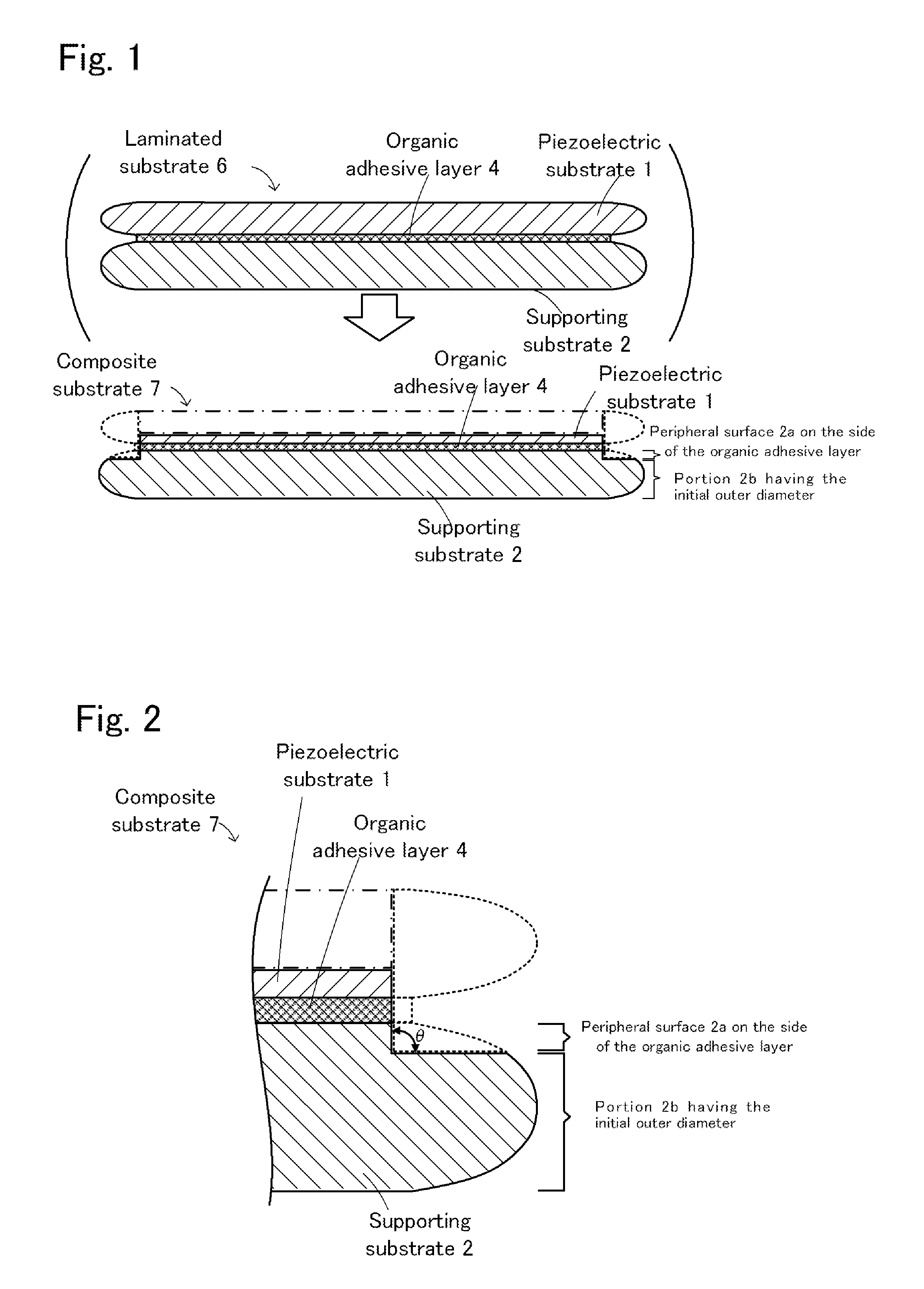
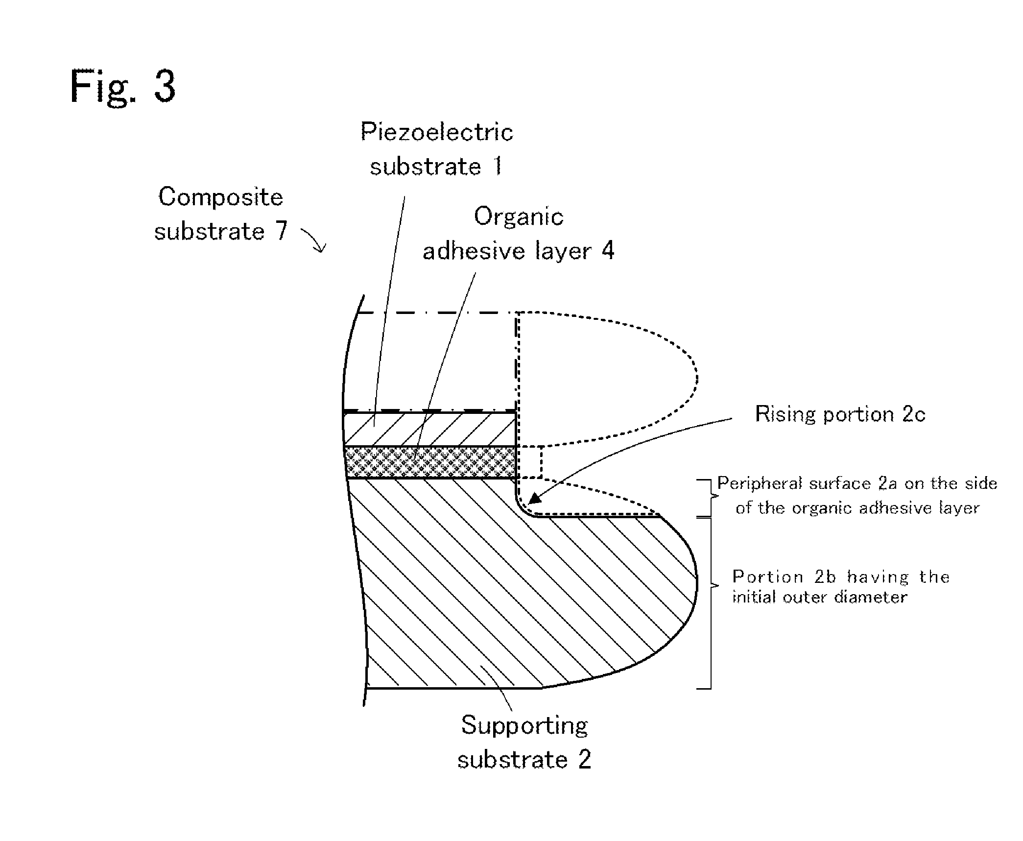
[0037]FIG. 4 shows schematic cross-sectional views of a manufacturing process of a composite substrate according to the present example. First, a lithium tantalate substrate (an LT substrate) 10 that had an orientation flat portion (an OF portion) and had a diameter of 100 mm and a thickness of 250 μl was prepared as a piezoelectric substrate. A silicon substrate 12 that had an OF portion and had a diameter of 100 mm and a thickness of 350 μm was prepared as a supporting substrate (FIG. 4(a)). The LT substrate 10 was a 36° Y-cut X-propagation LT substrate, in which X denotes the propagation direction of a surface acoustic wave (SAW), and 36° Y-cut denotes the cut angle of the substrate rotated about the X-axis with a rotational angle 36° from the Y-axis toward Z-axis. The LT substrate 10 and the silicon substrate 12 had a beveled edge. FIG. 5 is a fragmentary sectional view illustrating a bevel. As illustrated in the figure, the bevel extended from 300 μm inside a peripheral surface...

example 2

[0042]A hundred composite substrates were fabricated in the same way as in Example 1 except that the LT substrate 10 was a 42° Y-cut X-propagation LT substrate, that the thickness of the silicon substrate 12 was 250 μm, that the thickness of the organic adhesive layer 14 was 0.6 μm, and that the peripheral surface of the laminated substrate 16 was ground after the height of the grinding wheel 24 was adjusted such that the position of the undersurface of the whetstone 28 corresponded to the position 50 μm under the top of the silicon substrate 12. In all of the 100 composite substrates thus fabricated, the LT substrate 10 had no chip.

example 3

[0044]A hundred composite substrates were fabricated in the same way as in Example 1 except that the supporting substrate was formed of borosilicate glass. In all of the 100 composite substrates thus fabricated, the LT substrate 10 had no chip.


PUM

PropertyMeasurementUnit
thicknessaaaaaaaaaa
thicknessaaaaaaaaaa
thicknessaaaaaaaaaa

Abstract

A supporting substrate and a piezoelectric substrate are prepared. A surface of the supporting substrate is bonded to the backside of the piezoelectric substrate with an organic adhesive layer interposed therebetween to form a laminated substrate. Subsequently, a peripheral surface of the laminated substrate is ground such that a peripheral surface of the piezoelectric substrate, a peripheral surface of the organic adhesive layer, and a peripheral surface of the supporting substrate on the side of the organic adhesive layer are made flush with each other. Subsequently, the surface of the piezoelectric substrate is polished to reduce the thickness of the piezoelectric substrate and performing mirror polishing of the surface.

Description

BACKGROUND OF THE INVENTION[0001]1. Field of the Invention[0002]The present invention relates to a method for manufacturing a composite substrate and to a composite substrate.[0003]2. Description of the Related Art[0004]It is already known that a composite substrate, in which a supporting substrate and a piezoelectric substrate are bonded together, is provided with electrodes to fabricate elastic wave devices. For example, as elastic wave devices, surface acoustic wave devices and bulk acoustic wave devices have been used as band-pass filters in communication devices, such as mobile phones. Composite substrates are known to use lithium niobate or lithium tantalate as a piezoelectric substrate and silicon or quartz as a supporting substrate (see Patent Document 1).[Patent Document 1] Japanese Unexamined Patent Application Publication No. 2006-319679SUMMARY OF THE INVENTION[0005]Such composite substrates are often manufactured by preparing a piezoelectric substrate and a supporting su...

Claims


Application Information

Patent Timeline
Patent Type & Authority Applications(United States)
IPC IPC(8): H01L41/083H01L41/22H03H3/08H03H9/145
CPCY10T29/42H03H9/0585H01L41/337H01L41/313H10N30/073H10N30/086
Inventor SUZUKI, KENJIIWASAKI, YASUNORIYOSHINO, TAKASHI
Owner NGK INSULATORS LTD
Why Eureka
Try Eureka