Array, substrate, and display device and its manufacturing method

a technology of display devices and substrates, applied in the manufacture of electrode systems, electric discharge tubes/lamps, instruments, etc., can solve the problems of low resistance metal film likely to corrode under high temperature and high humidity environment, and the number of display panels obtained from one mother substrate is reduced, so as to improve the reliability of the display device

Active Publication Date: 2010-07-01
TRIVALE TECH
View PDF6 Cites 50 Cited by
  • Summary
  • Abstract
  • Description
  • Claims
  • Application Information

AI Technical Summary

Benefits of technology

[0011]The invention is also aimed at improving reliability of a display device that is assembled from the display panel having been cut and separated from the array substrate.

Problems solved by technology

In manufacturing steps prior to those of cutting and separating the array substrate and mounting a driver circuit and an external circuit, there has been a discharge breakdown problem that a short circuit or a break occurs in a scan wiring or a signal wiring formed on the array substrate owing to an external static electricity, or there has been a discharge breakdown problem of a gate insulation film that causes a change in characteristic such as a threshold level of the thin film transistor.
The short-wiring formed area to be disposed off are, as a matter of course, unusable for the display panel, which has caused a problem of reducing the number of display panels obtained from one mother substrate.
While scan wirings or signal wirings are generally formed of a metal film of low ohmic resistance, the low resistance metal film is likely to corrode under high temperature and high humidity environment.
For this reason, if the connection wirings are formed of such a low resistance metal film, corrosion occurs, depending upon a use environment of the display device, beginning from the connection wirings exposed on the cut end, and gradually progresses to the external-connection terminals of the array substrate and further to the leads, resulting in a reliability problem such as a malfunction due to a break in a wiring during operation of the display device.

Method used


Image

  • Array, substrate, and display device and its manufacturing method
  • Array, substrate, and display device and its manufacturing method
  • Array, substrate, and display device and its manufacturing method

Examples


embodiment 1

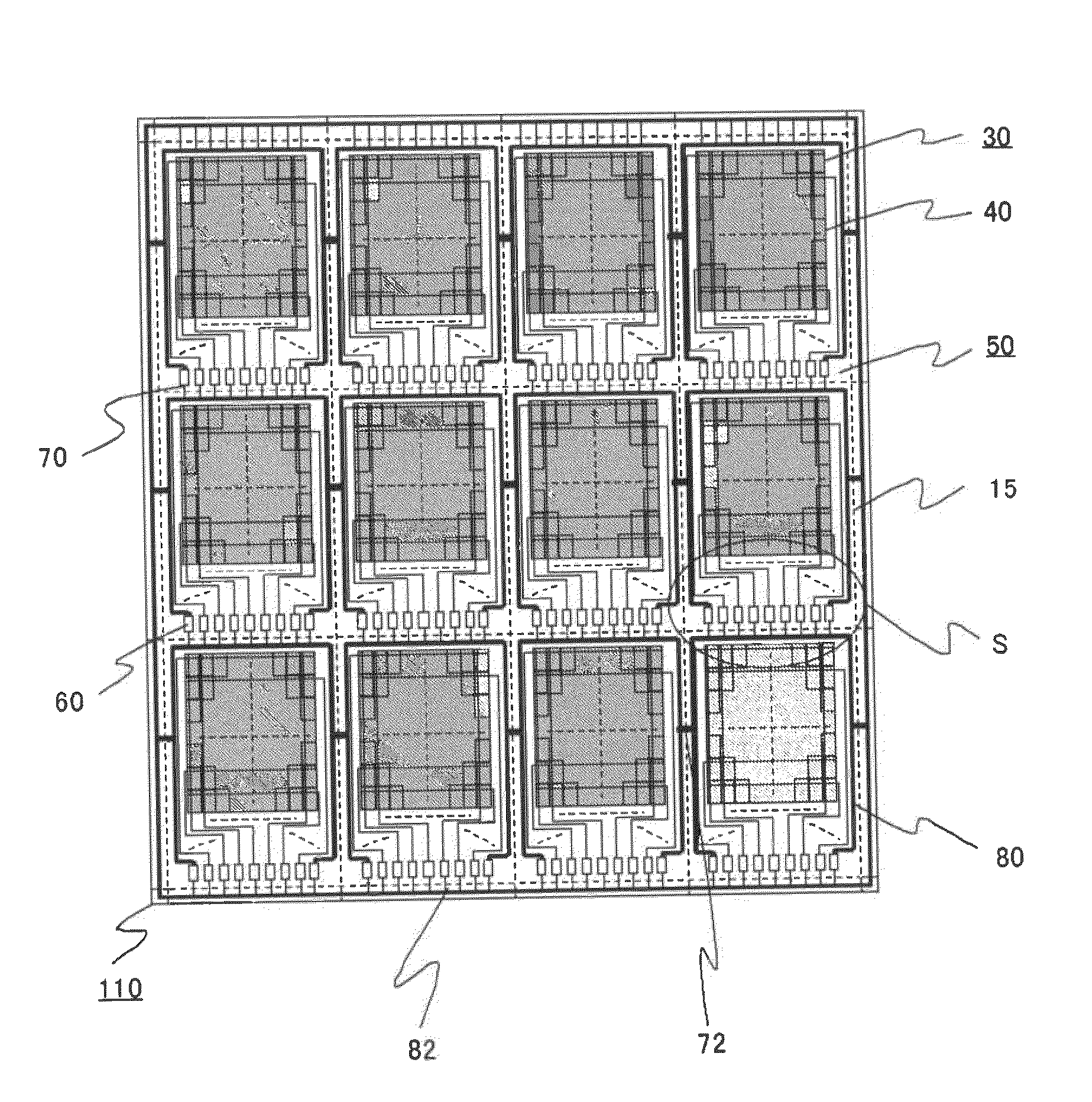
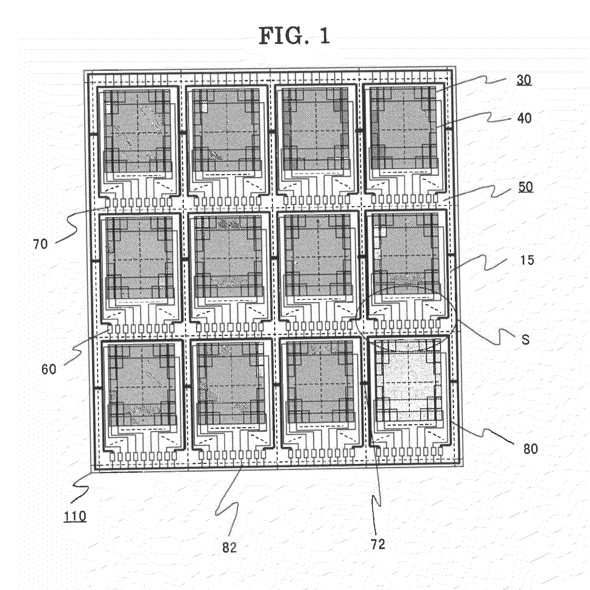
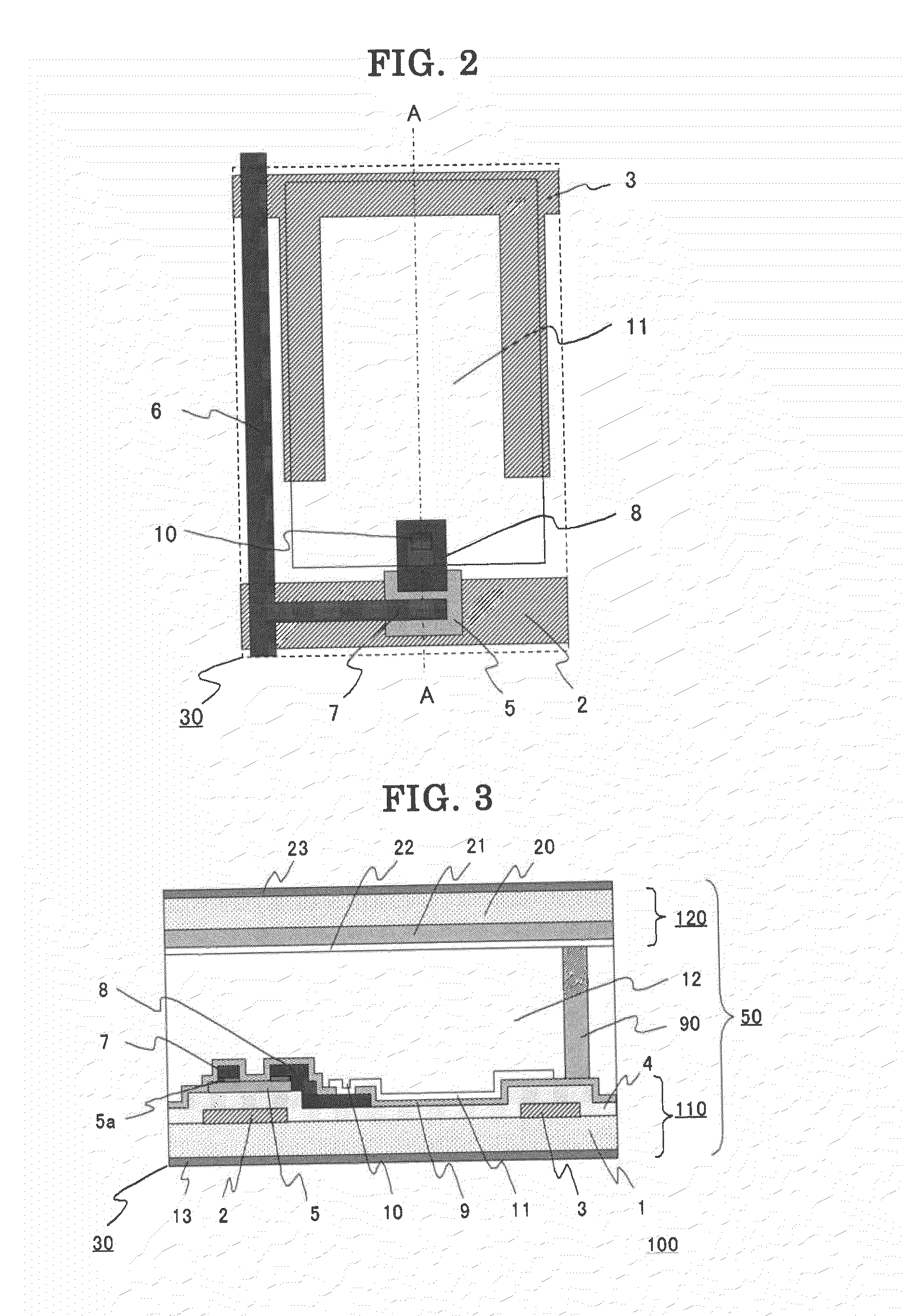
[0037]Embodiment 1 of the invention is a case of the display device being a liquid crystal display device. FIG. 1 is a plan view illustrating a schematic configuration of an array substrate of Embodiment 1, for a plurality of liquid crystal panels to be arranged thereon. FIG. 2 is an enlarged plan view illustrating one of pixels formed on the array substrate shown in FIG. 1, which constitute the display area of each liquid crystal panel. FIG. 3 is a cross-sectional view along the A-A line shown in FIG. 2. FIG. 4 is an enlarged plan view of a region S around a cutting line along which the array substrate is to be cut into the individual vertically-adjacent liquid crystal panels.

[0038]In FIGS. 1 to 3, an array substrate 110, on which formed is a plurality of display areas 40 (twelve panels, here) each having a plurality of pixels 30 arranged in a matrix, and an opposite substrate (color filter substrate) 120 are disposed facing to each other and spaced with a gap of approximately 2 to...

embodiment 2

[0067]FIG. 9 is an enlarged plan view illustrating an external-connection terminal portion L in Embodiment 2, for scan wirings. FIG. 10 is a cross-sectional view along the D-D line shown in FIG. 9. FIG. 11 is an enlarged plan view illustrating an external-connection terminal portion M or N in Embodiment 2, for signal wirings or a common wiring. FIG. 12 is a cross-sectional view along the E-E line shown in FIG. 11.

[0068]In Embodiment 1, the conductive film formed forming the signal wirings 6 is superior in corrosion resistance to that forming the scan wirings 2. In Embodiment 2, this relationship is revered, i.e., a conductive film forming scan wirings 2 is superior in corrosion resistance to that forming signal wirings 6. That is a case with, for example, the signal wirings 6 being made of a metal such as Al, Ag, Cu, or an alloy of any thereof, and the scan wirings 2 being made of a more corrosion-resistant metal such as Cr, Mo, Ti, Ta, W or an alloy of any thereof.

[0069]Firstly, a ...

embodiment 3

[0082]While in Embodiments 1 and 2 the common wiring 80 and the signal wirings 6 are formed from the same layer, in Embodiment 3 common wiring 80 and scan wirings 2 are formed from the same layer. The configurations of external-connection terminals 60 and connection wirings 70 are essentially the same as with Embodiments 1 and 2.

[0083]FIG. 13 is an enlarged cross-sectional view illustrating a transit portion (connecting portion) between a connection wiring and a common wiring both being formed from the same layer for scan wirings and the common wiring. FIG. 14 is an enlarged cross-sectional view illustrating another transit portion between the connection wiring and the common wiring both being formed from the same layer for the scan wirings.

[0084]In FIG. 13, a connection wiring 70 and the common wiring 80 of the adjacent liquid crystal panel 50 both being formed from the same layer for the scan wirings 2 are continuously connected directly with each other at the transit portion (con...


PUM


Abstract

An array substrate comprises on an insulative substrate, a plurality of display areas to be portions of a plurality of display panels, in which, each display area is constituted with a plurality of pixels arranged in a matrix, and the pixels is constituted with pixel electrodes formed at intersection portions of plural scan wirings and plural signal wirings; a common wiring is formed outside each display area, for applying a reference voltage to the pixels; a plurality of external-connection terminals is formed outside each display area, to be connected with a driver circuit that drives; and comprises connection wirings located so as to intersect a cutting line along which the insulative substrate is to be cut, for connecting the external-connection terminals in one of the display panels on the insulative substrate with a common wiring in another one of the display panels adjacent to the external-connection terminals, wherein the connection wirings are formed in a conductive layer superior in corrosion resistance to the most inferior corrosion-resistance conductive layer among conductive layers constituting the array substrate.

Description

FIELD OF THE INVENTION[0001]The present invention relates to an array substrate, and a display device and its manufacturing method. More particularly, the invention relates, in a case where a plurality of display panels, each being a major part of the display device, are formed on a mother substrate to form the array substrate, to an anti-static configuration of the array substrate on which formed are various wirings, thin film transistors, pixel electrodes, and the likes, and to an anti-corrosion configuration of the display device.BACKGROUND ART[0002]In recent years, display devices have been used in various apparatus as information display means for viewers. A new display panel (a major part of a display device, excluding an external circuit, a casing, and the like) that utilizes liquid crystal, plasma, electro-luminescence, field emission, or the like, becomes the mainstream of typical display devices now, in place of a Braun tube that was popularly utilized for display devices ...

Claims


Application Information

Patent Timeline
Patent Type & Authority Applications(United States)
IPC IPC(8): H05K1/03H01J9/20
CPCG02F1/133351G02F1/1345G02F1/136204G02F2001/136272H01L27/3276H01L2251/566H05K1/0254H05K3/0052G02F1/136272H10K59/131H10K71/851
Inventor TANAHARA, MANABU
Owner TRIVALE TECH
Why Eureka
Try Eureka