Group III nitride-based compound semiconductor light-emitting device

a compound semiconductor and light-emitting device technology, applied in the direction of semiconductor devices, basic electric elements, electrical equipment, etc., to achieve the effect of lowering the output efficiency of ligh

Active Publication Date: 2010-07-01
TOYODA GOSEI CO LTD
View PDF1 Cites 63 Cited by
  • Summary
  • Abstract
  • Description
  • Claims
  • Application Information

AI Technical Summary

Benefits of technology

[0007]In view of the foregoing, an object of the present invention is to prevent, in a Group III nitride-based compound semiconductor light-emitting device produced through a laser lift-off process and having an n-layer side serving as a light extraction side, from lowering an output efficiency of light on account of shield by the n-contact electrode.

Problems solved by technology

However, since the n-contact electrode formed on the light extraction side impedes light extraction, the design of the n-contact electrode leaves room for further improvement.

Method used


Image

  • Group III nitride-based compound semiconductor light-emitting device
  • Group III nitride-based compound semiconductor light-emitting device
  • Group III nitride-based compound semiconductor light-emitting device

Examples


example 1

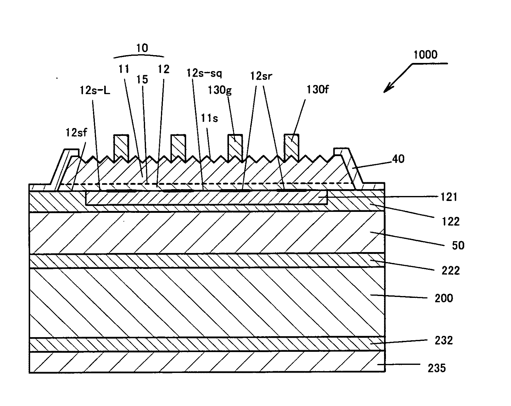
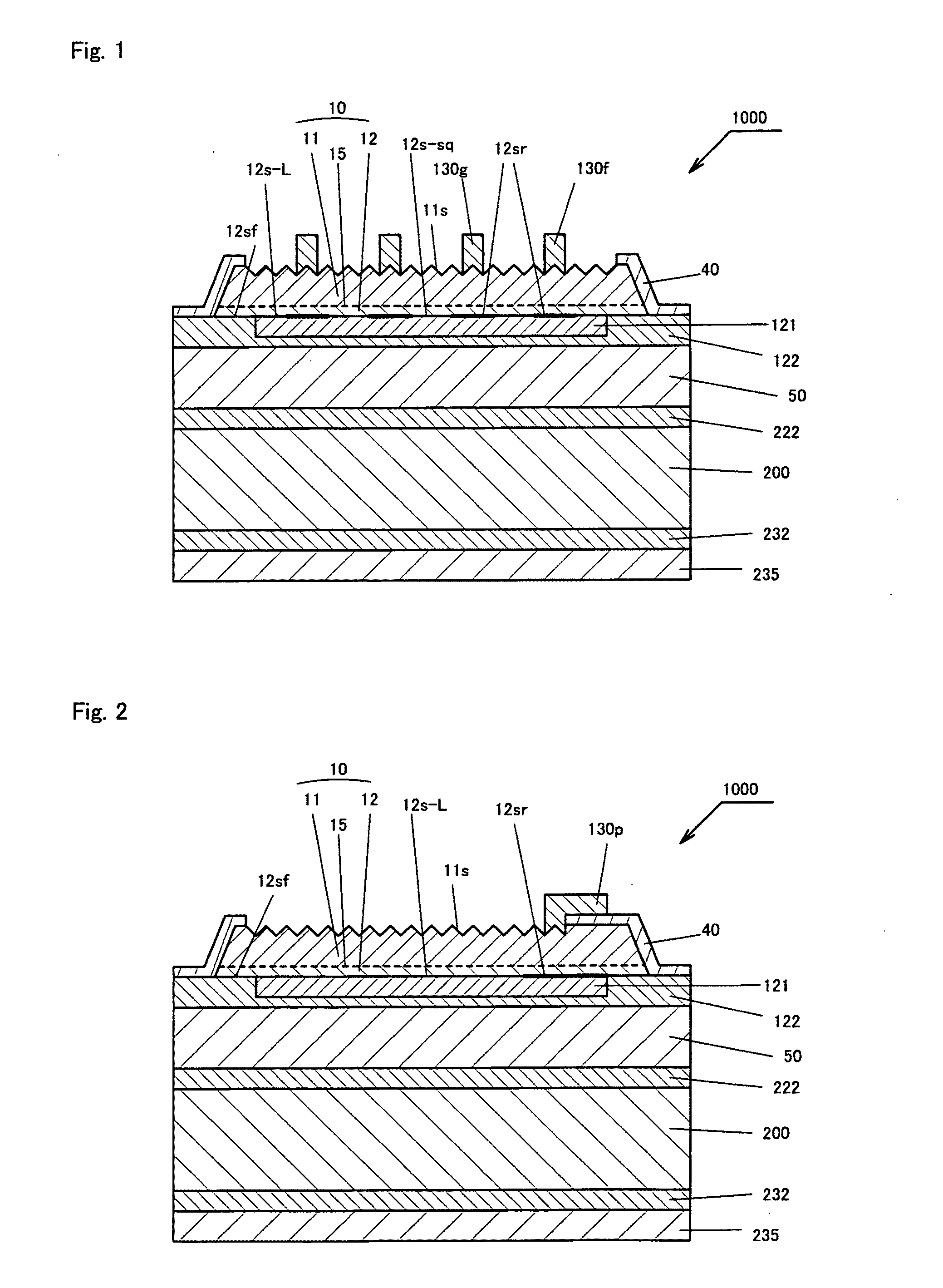
[0084]FIG. 1 is a cross-sectional view of the structure of a light-emitting diode (Group III nitride-based compound semiconductor light-emitting device) 1000 according to a specific example of the present invention, and FIG. 2 is another cross-sectional view of the light-emitting diode 1000. FIGS. 1 and 2 are cross-sectional views cut along line segments I-I and II-II, respectively, shown in FIG. 7 given hereinbelow.

[0085]The light-emitting diode 1000 shown in FIGS. 1 and 2 has a stacked structure having a p-type silicon substrate serving as a conductive support substrate 200 and, successively stacked on the support substrate 200, a conductive layer 222 formed of a plurality of stacked metal layers, a solder layer 50, a conductive layer 122 formed of a plurality of stacked metal layers, a p-contact electrode 121, a p-layer 12 formed mainly of a single layer or multiple layers of a p-type Group III nitride-based compound semiconductor, a light-emitting layer 15, an n-layer 11 formed ...

example 2

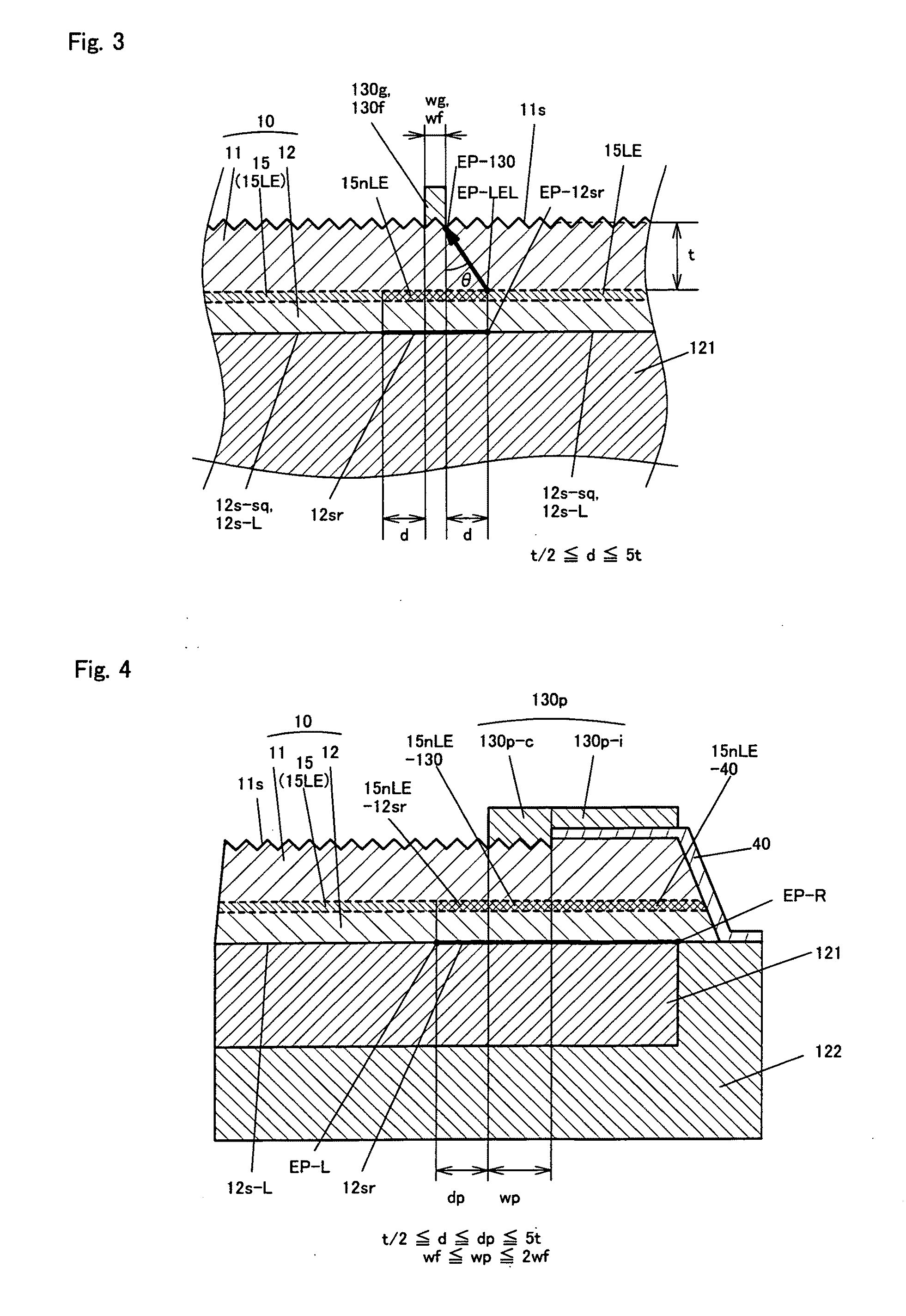
[0131]In Example 1, as shown in FIG. 5, the low-resistance face is divided by four belt-like areas of the high resistance face 12sr each having a width of 35 μm into nine low-resistance faces 12s-sq. The four belt-like areas of the high-resistance face 12sr each having a width of 35 μm may be replaced by low-resistance areas. Example 2 shows this feature.

[0132]FIG. 8 is a plan view of a light-emitting diode 2000 according to Example 2, showing the arrangement, on the side of a p-layer 12, with which a p-contact electrode 121 is contacted, of a high-resistance face 12sr′, low-resistance faces 12s-sq′ and 12s-L, and an outer peripheral surface 12sf which is not in ohmic contact with the p-contact electrode 121. The configuration shown in FIG. 8 differs from that in FIG. 5 in that the low-resistance face 12s-sq′ is a single square area (460 μm×460 μm) and that there are no grid-like areas in the high-resistance face 12sr′. Other than the two features, the configuration shown in FIG. 8 ...

example 3

[0135]Example 3 is directed to a light-emitting device in which at least a portion of a micro-embossed surface 11s of an n-layer 11 is right over the low-resistance faces 12s-sq and 12s-L of the p-layer 12 is covered with a transparent dielectric layer. FIG. 11 is a cross-sectional view showing the configuration of a light-emitting diode 3000 according to Example 3. The light-emitting diode 3000 shown in FIG. 11 is based on the configuration of the light-emitting diode 1000 according to Example 1 shown in FIG. 1 to which a transparent dielectric layer 45 has been added. FIG. 12 is another cross-sectional view of the light-emitting diode 3000 according to Example 3, which is almost equivalent to the cross-sectional view of FIG. 2, as viewed from a position different from that of the light-emitting diode 1000 according to Example 1 shown in FIG. 1.

[0136]As shown in FIGS. 11 and 12, in the light-emitting diode 3000, at least a portion of the micro-embossed surface 11s of the n-layer 11...


PUM


Abstract

In the Group III nitride-based compound semiconductor light-emitting device of the invention, an non-light-emitting area is formed in a light-emitting layer. In a light-emitting diode where light is extracted on the side of an n-layer, an outer wiring trace portion and an inner wiring trace portion of an n-contact electrode impedes light emission from the light-emitting layer. Therefore, there are provided, at the interface between a p-layer and a p-contact electrode, high-resistance faces having a width wider than the orthogonal projections of contact areas between the outer and inner wiring trace portions and the n-layer on the interface between the p-contact electrode and the p-layer. Through this configuration, current flow is limited, and portions having a total area equivalent to that of the high-resistance faces of the light-emitting layer serve as non-light-emitting areas. Thus, current can be supplied preferentially to an area of the light-emitting area where the outer wiring trace portion and the inner wiring trace portion are difficult to shade light, whereby light extraction efficiency with respect to supplied current can be enhanced.

Description

BACKGROUND OF THE INVENTION[0001]1. Field of the Invention[0002]The present invention relates to a Group III nitride-based compound semiconductor light-emitting device, and more particularly, to a Group III nitride-based compound semiconductor light-emitting device conductive in which a p-layer is joined to a conductive support substrate via a layer made of conductive material, and an n-layer is disposed on a light extraction side.[0003]The present invention is applicable to a light-emitting device produced through a so-called laser lift-off technique; i.e., a light-emitting device produced through epitaxially growing, on a hetero-substrate, a Group III nitride-based compound semiconductor, to thereby form a light-emitting device structure; bonding a conductive support substrate to the structure via a conductive layer made of metal, solder, or the like; and separating the hetero-substrate by irradiating, with laser light, the Group III nitride-based compound semiconductor thin layer...

Claims


Application Information

Patent Timeline
Patent Type & Authority Applications(United States)
IPC IPC(8): H01L33/00
CPCH01L33/0079H01L33/32H01L33/38H01L33/40H01L33/44H01L33/0093
Inventor UEMURA, TOSHIYAARAZOE, NAOKI
Owner TOYODA GOSEI CO LTD
Why Eureka
Try Eureka