Method of depositing tungsten film with reduced resistivity and improved surface morphology

a tungsten film and resistivity technology, applied in chemical vapor deposition coatings, coatings, metallic material coating processes, etc., can solve the problems of difficult uniform deposit of tungsten, poor film morphology of tungsten films comprised of thin tungsten nucleation layers and thick bulk tungsten layers, etc., to achieve the effect of improving surface morphology and reducing resistivity

Inactive Publication Date: 2010-07-01
APPLIED MATERIALS INC
View PDF20 Cites 37 Cited by
  • Summary
  • Abstract
  • Description
  • Claims
  • Application Information

AI Technical Summary

Problems solved by technology

There are, however, several disadvantages to depositing tungsten by traditional CVD methods.
Tungsten films comprised of a thin tungsten nucleation layer and a thick bulk tungsten layer tend to have poor film morphology.
Use of tungsten has frustrated photolithography steps during the manufacturing process as it results in a relatively rough surface having a reflectivity of 70% or less than that of silicon (thickness and wavelength dependent).
Also, tungsten has proven difficult to deposit uniformly, and poor surface uniformity typically increases film resistivity.
Traditional tungsten bulk deposition processes applying continuous flows of tungsten-containing gas, such as tungsten hexafluoride (WF6), and reducing gas, such as hydrogen (H2), on a tungsten nucleation layer are able to achieve low resistivity but result in high surface roughness.

Method used


Image

  • Method of depositing tungsten film with reduced resistivity and improved surface morphology
  • Method of depositing tungsten film with reduced resistivity and improved surface morphology
  • Method of depositing tungsten film with reduced resistivity and improved surface morphology

Examples


example

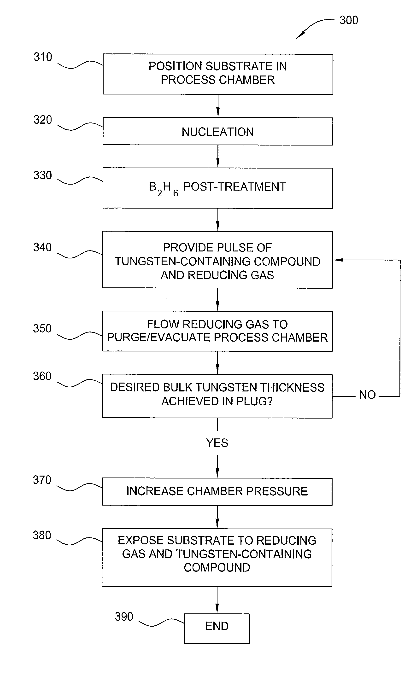
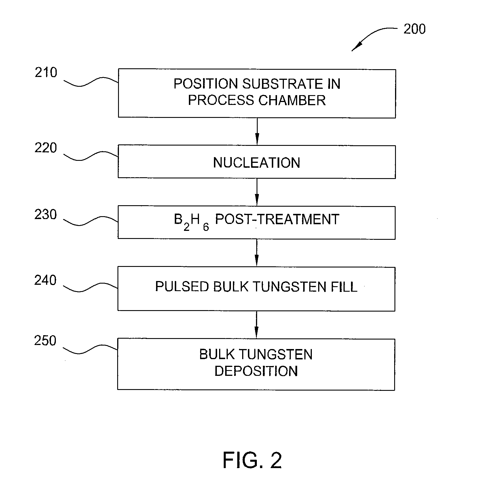
[0059]Following formation using a CVD process of a nucleation layer of desired thickness of about 30 angstroms using WF6 and B2H6 as reagents on a substrate having vias with a top critical dimension of about 50 nm and about a 4:1 aspect ratio, the substrate was maintained in the CVD chamber and a bulk tungsten layer was deposited using a two-stage deposition or fill method. In the first stage, a first bulk tungsten film was deposited to a thickness of about 500 angstroms in the vias under the following conditions:

Reagents: WF6 and H2;

Pressure: 90 Torr;

Temperature: 400° C.;

[0060]Flow rates: 100 sccm WF6 and 5,000 sccm H2;

Pulse Duration: 2 seconds.

The substrate was then maintained in the CVD chamber and the CVD chamber was pressurized to 300 Torr. During pressurization of the chamber, H2 was introduced at a flow rate of 3,000 sccm for about 20 seconds. During the second stage, a bulk tungsten layer was deposited to a thickness of 2,500 angstroms on the substrate surface using a CVD pr...


PUM

PropertyMeasurementUnit
temperatureaaaaaaaaaa
pressureaaaaaaaaaa
pressureaaaaaaaaaa

Abstract

A method of controlling the resistivity and morphology of a tungsten film is provided, comprising depositing a first film of a bulk tungsten layer on a substrate during a first deposition stage by (i) introducing a continuous flow of a reducing gas and a pulsed flow of a tungsten-containing compound to a process chamber to deposit tungsten on a surface of the substrate, (ii) flowing the reducing gas without flowing the tungsten-containing compound into the chamber to purge the chamber, and repeating steps (i) through (ii) until the first film fills vias in the substrate surface, increasing the pressure in the process chamber, and during a second deposition stage after the first deposition stage, depositing a second film of the bulk tungsten layer by providing a flow of reducing gas and tungsten-containing compound to the process chamber until a second desired thickness is deposited.

Description

CROSS-REFERENCE TO RELATED APPLICATIONS[0001]This application claims benefit of U.S. provisional patent application Ser. No. 61 / 141,988, filed Dec. 31, 2008, which is herein incorporated by reference.BACKGROUND OF THE INVENTION[0002]1. Field of the Invention[0003]Embodiments of the present invention generally relate to a method of tungsten film deposition, and more particularly, a method of forming a tungsten film with reduced resistivity and improved surface morphology.[0004]2. Description of the Related Art[0005]The semiconductor processing industry continues to strive for larger production yields while increasing the uniformity of layers deposited on substrates having larger surface areas. These goals, in combination with new materials, have led to higher integration of circuits per unit area of the substrate. As circuit integration increases, so does the need for greater uniformity and process control regarding thicknesses of layers deposited on substrates. As a result, various ...

Claims


Application Information

Patent Timeline
Patent Type & Authority Applications(United States)
IPC IPC(8): H01L21/768H01L21/3205
CPCC23C16/02C23C16/045C23C16/14C23C16/45523H01L21/28556H01L21/76861H01L21/76876H01L21/76877H01L21/205
Inventor WU, KAIKHANDELWAL, AMITGELATOS, AVERINOS V.
Owner APPLIED MATERIALS INC
Why Eureka
Try Eureka