Manufacturing method for silicon single crystal

a manufacturing method and silicon single crystal technology, applied in the direction of crystal growth process, polycrystalline material growth, under protective fluid, etc., can solve the problems of lowering the yield of silicon single crystal, and achieve the effect of reducing the introduction of dislocation

Active Publication Date: 2010-07-15
SUMCO TECHXIV
View PDF3 Cites 22 Cited by
  • Summary
  • Abstract
  • Description
  • Claims
  • Application Information

AI Technical Summary

Benefits of technology

[0029]According to the present invention, a manufacturing method for a silicon single crystal is provided that can reduce introduction of dislocati

Problems solved by technology

Here, as disclosed in Japanese Unexamined Patent Application Publication No. 2008-266093, it is known that a dopant should be added while growing a straight body portion of a silicon single crystal because a high concentration of dopant in the melt in growing of a shoulder portion to the

Method used


Image

  • Manufacturing method for silicon single crystal
  • Manufacturing method for silicon single crystal
  • Manufacturing method for silicon single crystal

Examples


first embodiment

Manufacturing Method of Silicon Single Crystal of First Embodiment of Present Invention

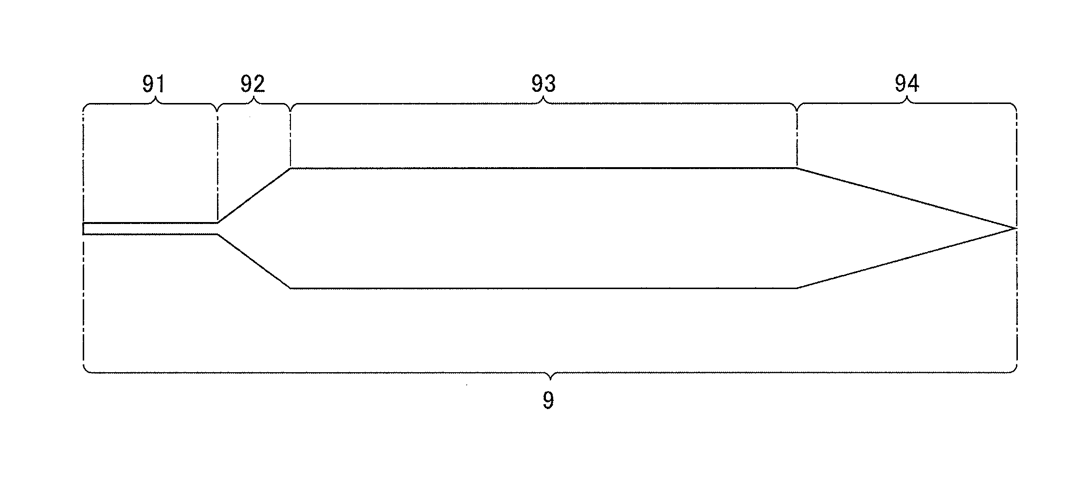
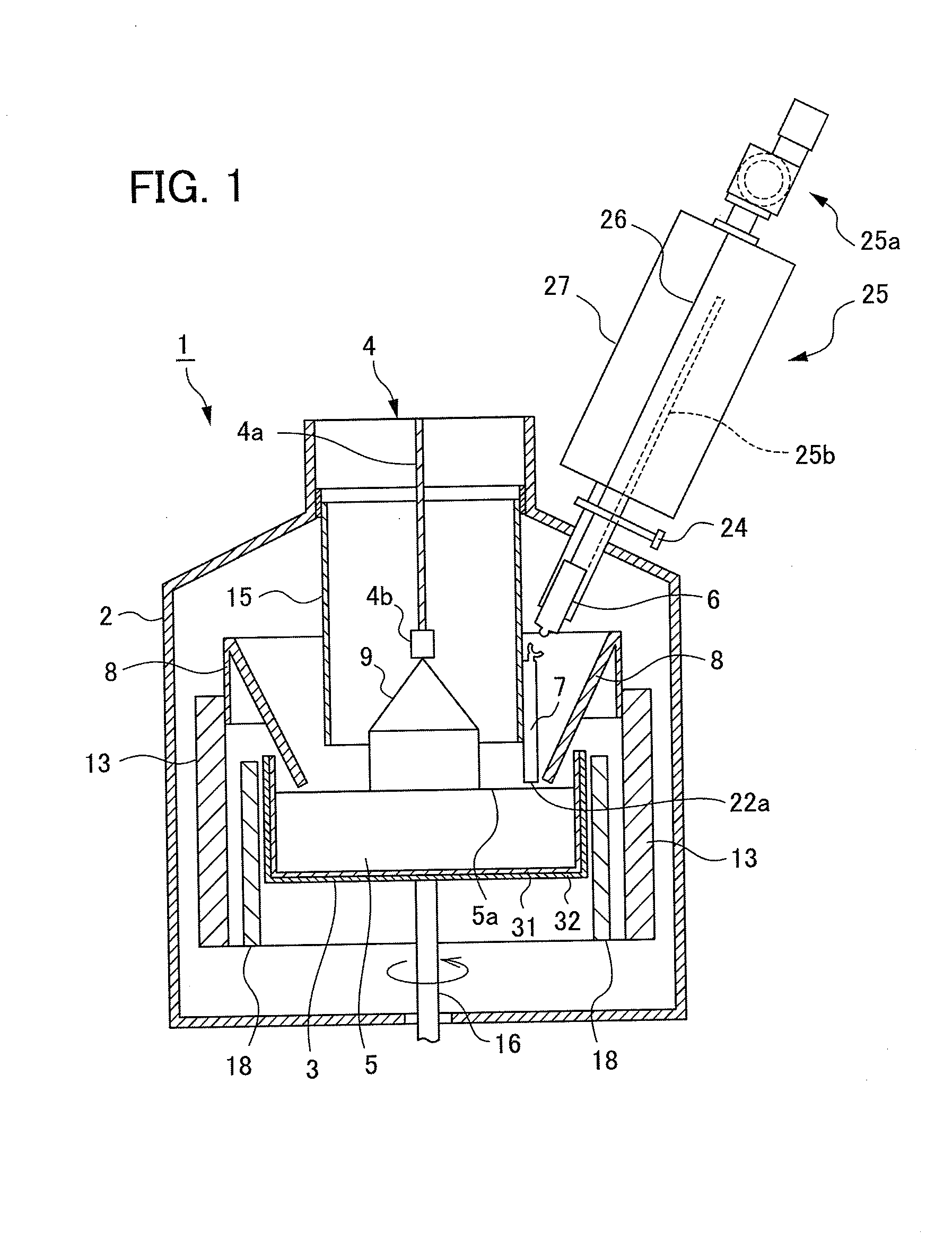
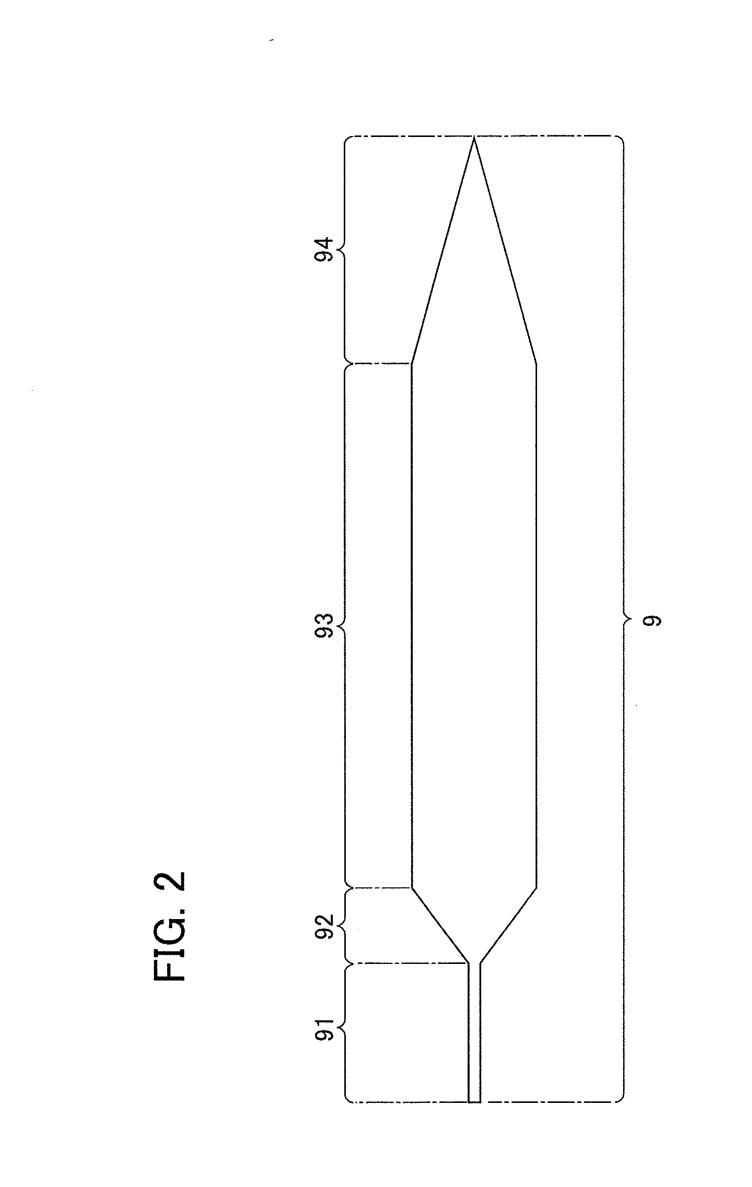
[0054]Next, a manufacturing method of the silicon single crystal according to the first embodiment of the present invention is described. The manufacturing method of the silicon single crystal according to the present embodiment can be divided into: a dipping step in which a seed crystal is dipped in the surface 5a of the melt 5; and a growth step in which the silicon single crystal 9 is grown by pulling the seed crystal dipped in the surface 5a of the melt 5 by the pulling mechanism 4. Each step is described hereinafter.

Dipping Step

[0055]First, the dipping step is described. This step is a step in which the seed crystal is dipped in the melt 5.

[0056]The seed crystal used in the dipping step is cut out from a silicon single crystal. The seed crystal may or may not include a substance as a dopant. In a case where a dopant is included in the seed crystal, the dopant is preferably the same type as th...

second embodiment

Manufacturing Method of Silicon Single Crystal of Second Embodiment of Present Invention

[0075]Next, a manufacturing method of a silicon single crystal according to the second embodiment of the present invention is described. In the manufacturing method of the silicon single crystal according to the second embodiment, introduction of dislocation into the silicon single crystal 9 is prevented not by controlling the addition rate of the dopant to the melt 5, but by controlling a decreasing rate of resistivity of the silicon single crystal 9 due to the addition of the dopant. It should be noted that a description of a part similar to the first embodiment, which has already been described, is omitted and differences from the first embodiment are mainly described.

[0076]As in the first embodiment, in the growth method of silicon single crystal according to the present embodiment, a dopant addition step is performed during growth of the straight body portion 93 in the growth step of the sil...

examples

[0137]The present invention is described in further detail hereinafter by way of examples; however, the present invention is not limited thereto.

[0138]One hundred kilograms of polycrystalline silicon as a raw material was put into a crucible and a melt was obtained, and 800 g of arsenic as a dopant was added thereto and then a silicon single crystal was pulled by the CZ method. Next, after pulling a shoulder portion of the silicon single crystal, i.e. while pulling a straight body portion, 40 g of arsenic as an additional dopant was added to the melt, as a dopant addition step. Addition of the dopant was performed by subliming the dopant stored in a sample tube by way of radiant heat from the melt, and blowing vapor thus obtained onto the melt. In the following Examples 1 to 3 and Comparative Examples 1 and 2, the addition rate of the dopant to the melt (a sublimation rate of the dopant) was adjusted by changing a distance between the sample tube and a surface of the melt. The addit...


PUM


Abstract

To provide a manufacturing method for a silicon single crystal that can reduce introduction of dislocation thereinto even if a required amount of dopant is added to a melt while growing a straight body portion of a silicon ingot. In a manufacturing method for a silicon single crystal according to the present invention that includes a dopant addition step of adding a dopant to a melt while a straight body portion of a silicon single crystal is growing in a growth step of growing the silicon single crystal by dipping a seed crystal into a silicon melt and then pulling the seed crystal therefrom, in the dopant addition step, a remaining mass of the melt is calculated at the beginning thereof, and the dopant is added to the melt at a rate of 0.01 to 0.035 g/min·kg per minute per 1 kg of the calculated remaining mass of the melt.

Description

[0001]This application is based on and claims the benefit of priority from Japanese Patent Application Nos. 2009-005919, 2009-005920 and 2009-007194, respectively filed on 14 Jan. 2009, 14 Jan. 2009, and 16 Jan. 2009, the contents of which are entirely incorporated herein by reference.BACKGROUND OF THE INVENTION[0002]1. Field of the Invention[0003]The present invention relates to a manufacturing method for a silicon single crystal, which grows a silicon single crystal by dipping a seed crystal into a silicon melt and then pulling the seed crystal therefrom. More particularly, the present invention relates to a manufacturing method for a silicon single crystal including a step of adding a dopant to the silicon melt while a straight body portion of the silicon single crystal is growing.[0004]2. Related Art[0005]The Czochralski method (CZ method) is a method that grows a silicon single crystal by dipping a seed crystal into a silicon melt and then pulling the seed crystal therefrom. In...

Claims


Application Information

Patent Timeline
IPC IPC(8): C30B15/04
CPCC30B29/06C30B15/04
Inventor NARUSHIMA, YASUHITOKUBOTA, TOSHIMICHIKAWAZOE, SHINICHIOGAWA, FUKUOFUKUDA, TOMOHIRO
Owner SUMCO TECHXIV
Why Eureka
Try Eureka