Plasma display panel

Inactive Publication Date: 2010-07-15
PANASONIC CORP
View PDF5 Cites 0 Cited by
  • Summary
  • Abstract
  • Description
  • Claims
  • Application Information

AI Technical Summary

Benefits of technology

[0021]The present invention addresses these problems, and provides a PDP that sufficiently removes impu

Problems solved by technology

However, it is difficult to completely exhaust all gases including the impure gas adsorbed in the PDP, and some impure gas inevitably remains inside the PDP.
However, it is known that the material of the protective layer or phosphor reacts with the impure gas and its characteristic degrades.
Especially, much water remaining inside the PDP adversely affects the discharge characteristic of the protective layer, reduces the breakdown voltage of the discharge cells, and causes a “bleeding” degradation of the image qual

Method used


Image

  • Plasma display panel
  • Plasma display panel
  • Plasma display panel

Examples


Example

First Exemplary Embodiment

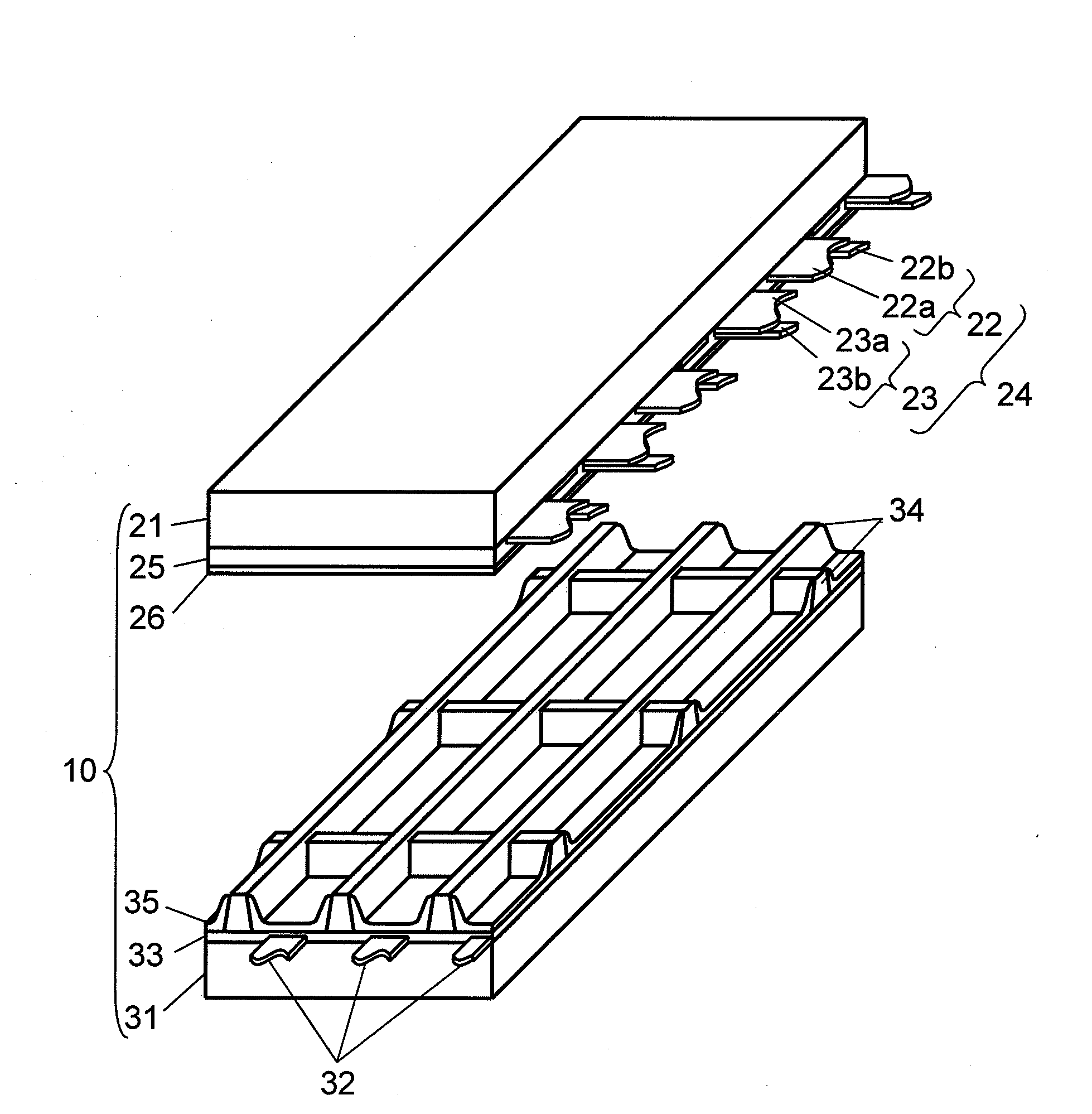
[0041]FIG. 1 is an exploded perspective view showing a structure of a PDP in accordance with a first exemplary embodiment of the present invention. FIG. 2 is a sectional view of the PDP in accordance with the first exemplary embodiment of the present invention. PDP 10 is formed by sticking glass-made front substrate 21 to rear substrate 31. A plurality of display electrode pairs 24 formed of scan electrodes 22 and sustain electrodes 23 are disposed on front substrate 21. Dielectric layer 25 is formed so as to cover display electrode pairs 24, and protective layer 26 is formed on dielectric layer 25. A plurality of data electrodes 32 are formed on rear substrate 31, dielectric layer 33 is formed so as to cover data electrodes 32, and mesh barrier rib 34 is formed on dielectric layer 33. Phosphor layer 35 for emitting lights of respective colors of red, green, and blue is formed on the side surfaces of barrier rib 34 and on dielectric layer 33.

[0042]In the fi...

Example

Second Exemplary Embodiment

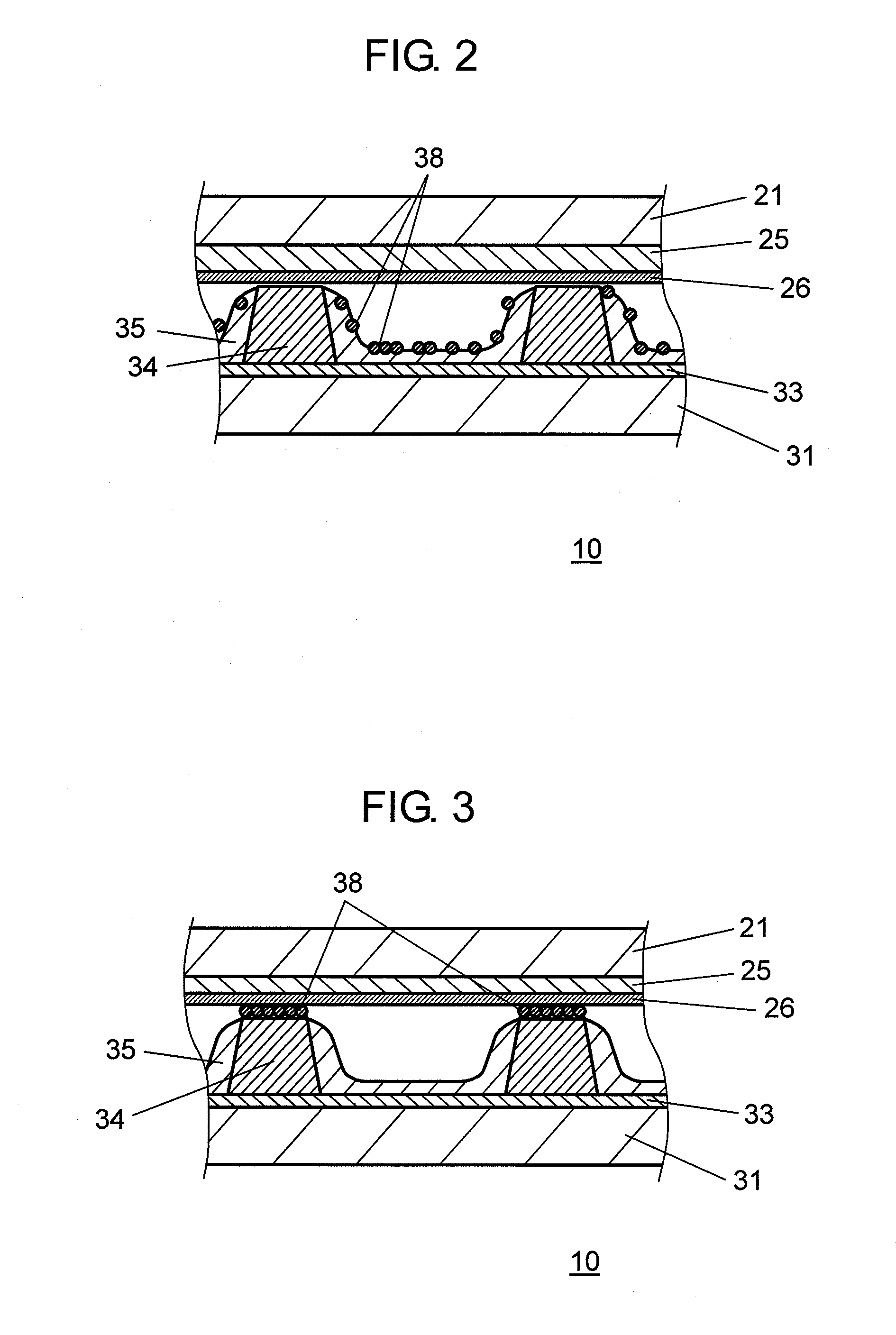
[0055]PDP 10 of the second exemplary embodiment of the present invention differs from the first exemplary embodiment in that hydrogen-absorbing materials 38 are disposed on the surface of barrier rib 34, especially on the top of barrier rib 34, in the second exemplary embodiment. FIG. 3 is a sectional view of the PDP 10 in accordance with the second exemplary embodiment of the present invention, and schematically shows hydrogen-absorbing materials 38 that are disposed on the top of barrier rib 34.

[0056]The grain size of the platinum-group powder used as hydrogen-absorbing materials 38 in the second exemplary embodiment must be set so that a large distance does not occur between barrier rib 34 and protective layer 26, and is preferably 0.1 to 5 μm. The thickness of the platinum-group powder layer is also preferably 5 μm or smaller, and the platinum-group powder may be simply interspersed on the top of barrier rib 34.

[0057]Hydrogen-absorbing materials 38 are...

Example

Third Exemplary Embodiment

[0058]PDP 10 of the third exemplary embodiment of the present invention differs from the first exemplary embodiment in that hydrogen-absorbing materials 38 are disposed on protective layer 26 of front substrate 21 in the third exemplary embodiment. FIG. 4 is a sectional view of PDP 10 in accordance with the third exemplary embodiment of the present invention, and schematically shows hydrogen-absorbing materials 38 dispersed on protective layer 26.

[0059]Similarly to the second exemplary embodiment, the grain size of the platinum-group powder used as hydrogen-absorbing materials 38 in the third exemplary embodiment must be set so that a large distance does not occur between barrier rib 34 and protective layer 26, and is preferably 0.1 to 5 μm. The coverage factor at which the platinum-group powder covers protective layer 26 is preferably set to 50% or lower so as to prevent the platinum-group powder from disturbing the transmission of visible light.


PUM


Abstract

A plasma display panel has a front substrate including a plurality of display electrode pairs, a dielectric layer, and a protective layer, and a rear substrate including a plurality of data electrodes, a barrier rib, and a phosphor layer. The front substrate and rear substrate are faced to each other so that the display electrode pairs and the data electrodes intersect, and a hydrogen-absorbing material containing palladium inside is disposed.

Description

TECHNICAL FIELD[0001]The present invention relates to a plasma display panel used for image display.BACKGROUND ART[0002]Recently, a plasma display panel (hereinafter referred to as “PDP”) has received attention as a color display device capable of having a large screen and being thin and light in weight.[0003]An AC surface discharge type PDP typical as a PDP has many discharge cells between a front substrate and a rear substrate that are faced to each other. The front substrate has the following elements:[0004]a plurality of display electrode pairs disposed in parallel on a glass substrate; and[0005]a dielectric layer and a protective layer that are formed so as to cover the display electrode pairs.Here, each display electrode pair is formed of a pair of scan electrode and sustain electrode. The protective layer is a thin film made of alkali earth oxide such as magnesium oxide (MgO), protects the dielectric layer from ion spatter, and stabilizes the discharge characteristic such as ...

Claims


Application Information

Patent Timeline
IPC IPC(8): H01J17/49H01J9/02H01J9/227H01J11/12H01J11/22H01J11/24H01J11/26H01J11/34H01J11/36H01J11/38H01J11/40H01J11/42H01J11/50H01J11/52
CPCH01J11/52H01J11/12H01J11/36H01J11/40H01J11/42
Inventor SOGOU, HIROSHIOKUMURA, SHIGEYUKI
Owner PANASONIC CORP
Why Eureka
Try Eureka