Method of improving nanotopography of surface of wafer and wire saw apparatus

a technology of wire saw and surface, which is applied in the field of improving the nanotopography of the surface of the wafer and wire saw apparatus, can solve the problems of nanotopography sensory test rejection, the size of the surface waviness component called a “nanotopography” is a problem, and the numerical value judgment of nanotopography, so as to improve the straightness of the feed of the work feed table, improve the surface nanotopography, and eliminate the effect of cutting

Active Publication Date: 2010-07-22
SHIN-ETSU HANDOTAI CO LTD
View PDF5 Cites 7 Cited by
  • Summary
  • Abstract
  • Description
  • Claims
  • Application Information

AI Technical Summary

Benefits of technology

[0007]It is an object of the present invention to provide a method of eliminating slice waviness having periodicity to improve nanotopography of a surface of a wafer and a wire saw apparatus.
[0008]To achieve this object, according to the present invention, there is provided a method of improving nanotopography of a surface of a wafer sliced from an ingot by using a wire saw apparatus, at least including improving straightness of feed of a work feed table which is included in the wire saw apparatus and used for feeding the ingot to a wire row formed by winding a wire around a plurality of rollers.
[0009]Improving the straightness of feed of the work feed table for feeding the ingot to the wire row in this manner enables eliminating slice waviness having periodicity and improving the nanotopography of the wafer surface.

Problems solved by technology

On the other hand, a size of a surface waviness component called a “nanotopography” is a problem in wafers in recent years.
It is said that this nanotopography affects a yield of an STI (Shallow Trench Isolation) step in device manufacture.
Of these nano-topographies, it can be considered that the “one which extemporaneously occurs” is caused due to wire disconnection or an error in tension control of the wire saw apparatus, whilst the “one which occurs at start or end of slicing” is caused due to a sudden change in a cut-resistance, often resulting in rejection in nanotopography numerical value judgment.
On the other hand, the “waviness having periodicity” often results in rejection in nanotopography sensory test, but its cause is unknown.

Method used


Image

  • Method of improving nanotopography of surface of wafer and wire saw apparatus
  • Method of improving nanotopography of surface of wafer and wire saw apparatus
  • Method of improving nanotopography of surface of wafer and wire saw apparatus

Examples


example 1

Comparative Example 1

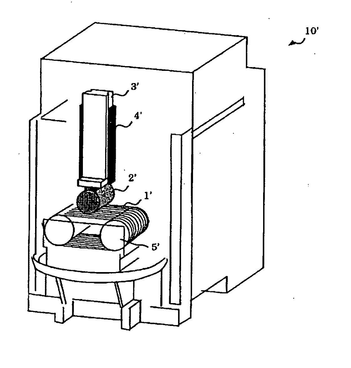
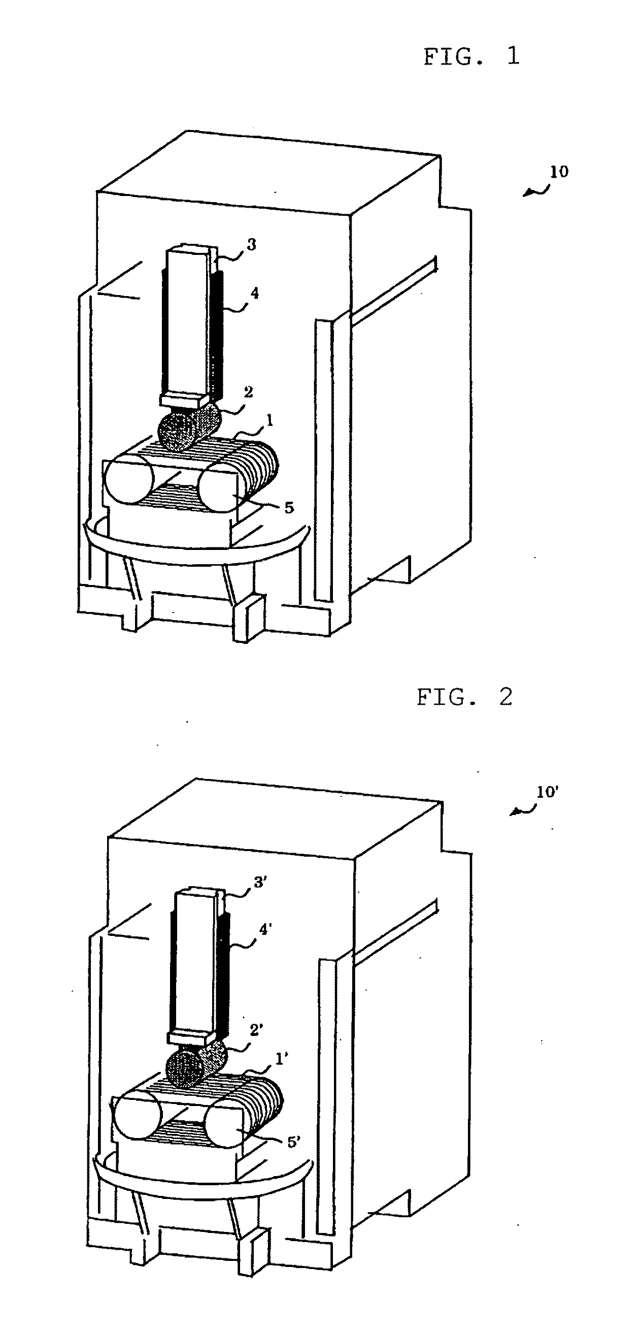
[0046]In the wire saw apparatus shown in FIG. 1, intervals of attachment holes which are used to attach an LM guide to the wire saw apparatus by using the bolts and tightening torque of bolts were respectively adjusted from 100 mm and 60 Nm (Comparative Example 1) to 75 mm and 40 Nm (Example 1) like the above-explained simulation. Further, straightness of feed of the work feed table was measured by the same method as above.

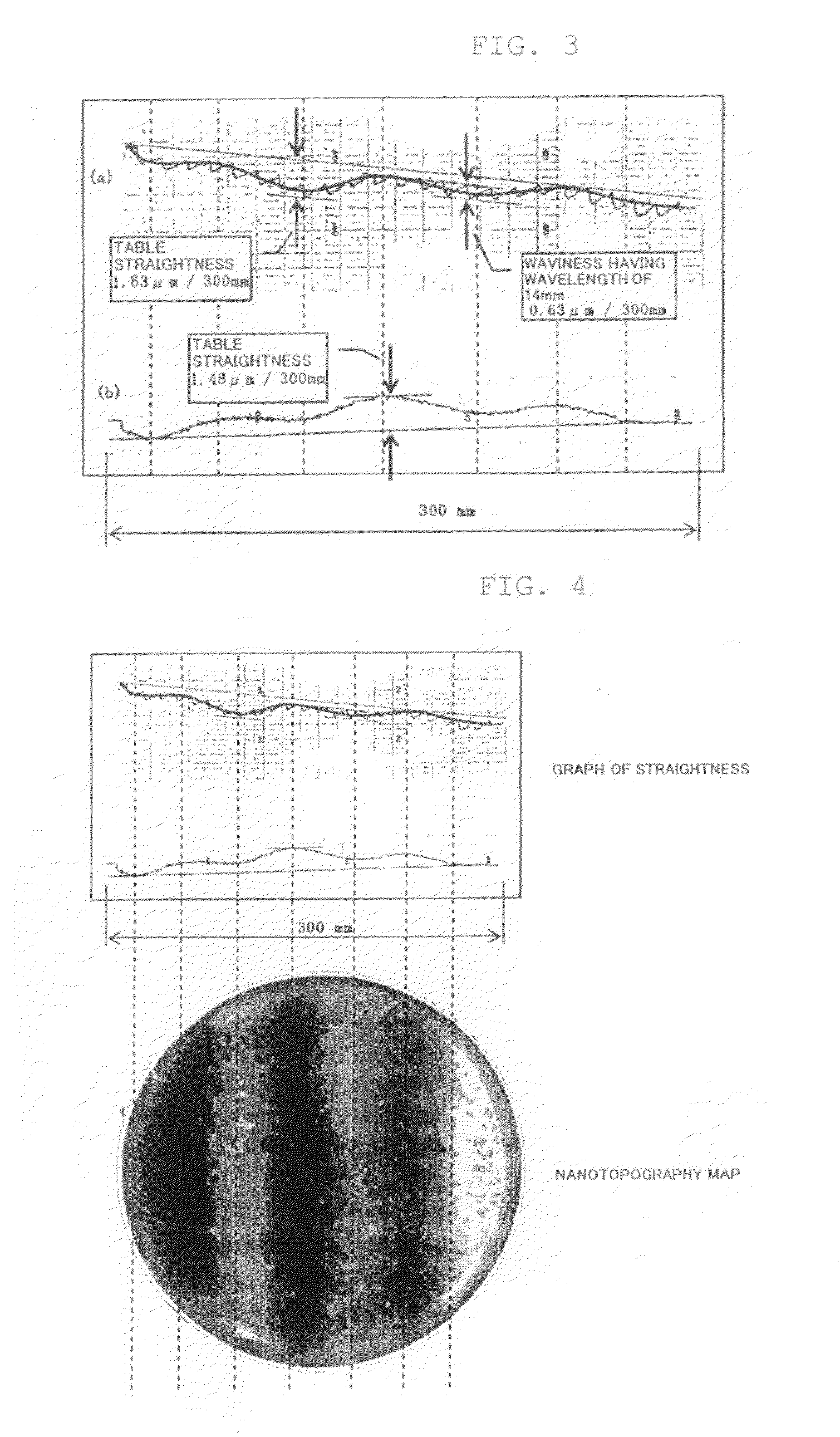
[0047]As a result, while straightness of feed of the work feed table was 1.48 μm / 300 mm and a component having a wavelength of approximately 100 mm was 1.48 μm in terms of a PV value in Comparative Example 1, straightness of feed of the work feed table was 0.92 μm / 300 mm and a component having a wavelength of approximately 100 mm was 0.92 μm in terms of the PV value in Example 1 as shown in FIG. 6, thereby providing the wire saw apparatus having the greatly improved straightness of feed of the work feed table. Based on a result depicted in FIG...

example 2

Comparative Example 2

[0048]The wire saw apparatuses in Example 1 and Comparative Example 1 were utilized to slice a silicon ingot having a diameter of 300 mm under conditions whose an outline is shown in Table 1, and the sliced ingots were polished to obtain silicon wafers (Example 2, Comparative Example 2). FIG. 7 shows a typical example of nanotopography map of the polished silicon wafer according to Example 2. Moreover, Table 2 shows N numbers of the wafers and frequencies of occurrence of “slice waviness having periodicity” as a problem with a frequency of occurrence in Comparative Example 2 being determined as 100%. The frequency of occurrence of “slice waviness having periodicity” in Example 2 was improved to approximately 1 / 10 of that in Comparative Example 2 by improving straightness of feed of the work feed table carried out in Example 1.

TABLE 1ItemConditionWorkIngot diameter300mmWireWire diameter160μmWire tension2.8kgfNew wire line supply amount100m / minWire reversal cycle6...


PUM

PropertyMeasurementUnit
wavelengthaaaaaaaaaa
speedaaaaaaaaaa

Abstract

The present invention provides a method of improving nanotopography of a surface of a wafer sliced from an ingot by using a wire saw apparatus, including improving straightness of feed of a work feed table which is included in the wire saw apparatus and used for feeding the ingot to a wire row formed by winding a wire around a plurality of rollers, and also provides a wire saw apparatus for slicing an ingot to manufacture a wafer, including: a wire row formed by winding a wire around a plurality of rollers; a work feed table for holding and feeding the ingot to the wire row; and a linear-motion guide for linearly guiding the work feed table, wherein a component having a wavelength of 20 to 200 mm in straightness of feed of the work feed table satisfies a PV value ≦1.0 μm. As a result, there are provided the method of eliminating slice waviness having periodicity to improve the nanotopography of the surface of the wafer and the wire saw apparatus.

Description

TECHNICAL FIELD[0001]The present invention relates to a method of improving nanotopography of a surface of a wafer, e.g., a silicon wafer or a compound semiconductor wafer sliced from an ingot by using a wire saw apparatus, and to a wire saw apparatus.BACKGROUND ART[0002]For example, when manufacturing a silicon wafer, a single-crystal silicon ingot is sliced by using a wire saw apparatus (see, e.g., Japanese Patent Application Laid-open No. 85053-1996). The wire saw apparatus is an apparatus which enables a wire (a high-tension steel wire) to travel at a high speed and presses an ingot against the wire to be sliced (cut) while applying a slurry having GC (silicon carbide) abrasive grains dispersed in a liquid to the wire. As an apparatus for slicing an ingot, one which applies a tension of 2.5 to 3.0 kgf to a wire having a diameter of 0.14 mm to 0.18 mm and performs slicing while enabling the wire to travel in a reciprocating direction at an average speed of 400 to 500 m / min in a c...

Claims


Application Information

Patent Timeline
Patent Type & Authority Applications(United States)
IPC IPC(8): B28D5/04
CPCB23D57/0046B28D5/045B28D5/0082B24B27/0633B24B27/06B24B47/04B28D5/04B82Y10/00
Inventor OISHI, HIROSHIKATO, TADAHIRO
Owner SHIN-ETSU HANDOTAI CO LTD
Why Eureka
Try Eureka