Semiconductor device and manufacturing method of the same

a semiconductor and manufacturing method technology, applied in the direction of semiconductor devices, semiconductor/solid-state device details, electrical devices, etc., can solve the problems of more fragile structure and porous low-k materials, and achieve the effect of small blade width

Inactive Publication Date: 2010-07-22
RENESAS ELECTRONICS CORP
View PDF2 Cites 42 Cited by
  • Summary
  • Abstract
  • Description
  • Claims
  • Application Information

AI Technical Summary

Benefits of technology

[0012]The present inventors have also found that when the dicing blade has a side face in a perpendicular direction to the surface (main surface) of the semiconductor wafer, a large cutting stress occurs also in a contact region between the low-k layer and the side face of the dicing blade during insertion of the dicing blade into the semiconductor wafer, which may easily cause cracks in the low-k layer.
[0013]Thus, when cracks appear in the low-k layer, they may presumably propagate even into a device region adjacent to a dicing region and deteriorate the reliability of the semiconductor device.
[0016]When the dicing blade is brought into contact with the surface (main surface) of the semiconductor wafer, employing such a structure enables to limit the contact between a dicing blade and the surface of the semiconductor wafer to only a contact between a portion of the cutting face of the dicing blade and the surface (main surface) of the semiconductor wafer. In short, employing such a structure enables to reduce a contact region between the dicing blade and the semiconductor wafer. As a result, a cutting stress generated when the dicing blade is inserted into the semiconductor wafer can be reduced so that cracks can be suppressed even if the dicing blade reaches a low-k layer.
[0019]One of the objects of the invention is to suppress occurrence of cracks in a semiconductor wafer having a low-k layer (improvement in cutting property).
[0021]A further object of the invention is to improve the life of a dicing blade.
[0026]In the manufacturing method of a semiconductor device having a multi-level interconnect layer containing a low-k layer, when a semiconductor wafer is subjected to a step cut dicing treatment in which a groove is formed with a tapered blade (first dicing blade) and then, the groove is divided with a straight blade (second dicing blade) having a blade width smaller than the width of the groove, the multi-level interconnect layer portion is cut while being covered with a tapered face and then, the wafer is separated with the blade that has a small blade width and is not contiguous to that portion so that dicing is performed without give damage to a relatively fragile low-k layer.

Problems solved by technology

Porous low-k materials, on the other hand, have a more fragile structure than materials constituting insulating layers of a conventional structure (non-porous materials) because insulating layers comprised of the porous low-k materials have therein many clearances (voids).

Method used


Image

  • Semiconductor device and manufacturing method of the same
  • Semiconductor device and manufacturing method of the same
  • Semiconductor device and manufacturing method of the same

Examples


Embodiment Construction

[0056][Outline of Embodiments] First, the outline of typical embodiments of the invention disclosed herein will be described.

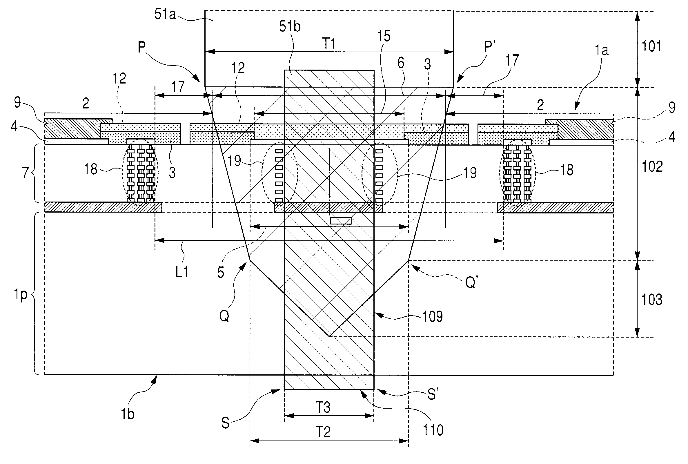
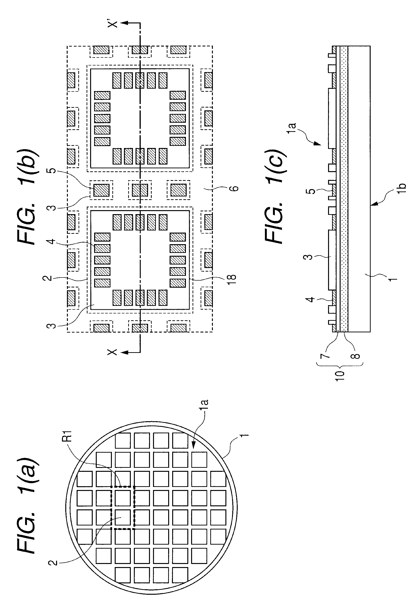
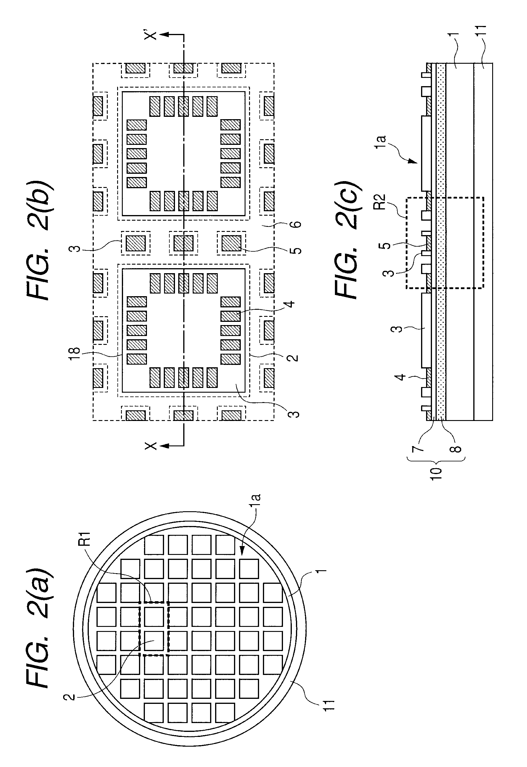
[0057]1. A manufacturing method of a semiconductor device comprising the steps of: (a) preparing a semiconductor wafer having a main surface, a plurality of device regions formed over the main surface, a dicing region formed between the device regions, and a back surface on a side opposite to the main surface; (b) in the dicing region of the semiconductor wafer, inserting a first dicing blade into the semiconductor wafer from the main surface side to the back surface side of the semiconductor wafer and causing the first dicing blade to run along the dicing region, thereby forming a dicing groove in the main surface of the semiconductor wafer (or dicing the main surface); (c) after the step (b), inserting a second dicing blade into the dicing groove from the main surface side of the semiconductor wafer and causing the second dicing blade to run along the dicing...


PUM

PropertyMeasurementUnit
end-face angleaaaaaaaaaa
dielectric constantaaaaaaaaaa
angleaaaaaaaaaa

Abstract

With a recent shrinking semiconductor process, insulating layers formed between interconnect layers are becoming thin. To avoid parasitic capacitance between them, materials of a low dielectric constant have been used for an insulating layer in a multilevel interconnect. Low-k materials, however, have low strength compared with the conventional insulating layers. Porous low-k materials are structurally fragile. The invention therefore provides a manufacturing method of a semiconductor device having a multilevel interconnect layer including a low-k layer. According to the method, in a two-step cutting system dicing in which after formation of a groove in a semiconductor water with a tapered blade, the groove is divided with a straight blade thinner than the groove width, the multilevel interconnect layer portion is cut while being covered with a tapered face and then the wafer is separated with a thin blade which is not brought into contact with the multilevel interconnect layer portion. The wafer can be diced without damaging a relatively fragile low-k layer.

Description

CROSS-REFERENCE TO RELATED APPLICATIONS[0001]The disclosure of Japanese Patent Application No. 2009-11570 filed on Jan. 22, 2009 including the specification, drawings and abstract is incorporated herein by reference in its entirety.BACKGROUND OF THE INVENTION[0002]The present invention relates to the structure of a semiconductor device (or a semiconductor integrated circuit device) or a technology effective when applied to a dicing technology in a manufacturing method of a semiconductor device (or a semiconductor integrated circuit device).[0003]Japanese Unexamined Patent Publication No. 2008-55519 (Patent Document 1) discloses a technology of cutting an optical IC structure, which has been obtained by attaching a relatively soft prism layer comprised of an optical glass onto an optical IC substrate comprised of a relatively hard silicon material, with a rotary blade so as not to make cracks in the structure. Described specifically, according to this technology, a portion of the upp...

Claims


Application Information

Patent Timeline
Patent Type & Authority Applications(United States)
IPC IPC(8): H01L23/522H01L21/304H01L21/56
CPCB28D5/022H01L21/78H01L23/3121H01L2224/48095H01L2224/48247H01L2224/48465H01L24/48H01L2924/01029H01L2924/01078H01L2924/01079H01L2924/10157H01L2924/10253H01L2924/01019H01L2924/01013H01L2924/00014H01L2924/00H01L2924/181H01L2224/05554H01L2924/10156H01L2924/14H01L24/49H01L2224/49171H01L2924/10155H01L2924/00012H01L2224/45099H01L2224/45015H01L2924/207H01L21/304H01L21/30625
Inventor AKIBA, TOSHIHIKOKIMURA, MINORUODAGIRI, MASAO
Owner RENESAS ELECTRONICS CORP
Why Eureka
Try Eureka