

Semiconductor device
a technology of semiconductor devices and contact wires, applied in semiconductor devices, diodes, electrical apparatus, etc., can solve the problems of disadvantages and drain wires, and achieve the effect of improving the connection reliability of contact wires
- Summary
- Abstract
- Description
- Claims
- Application Information
AI Technical Summary
Benefits of technology
Problems solved by technology
Method used
Image

Examples
example 1
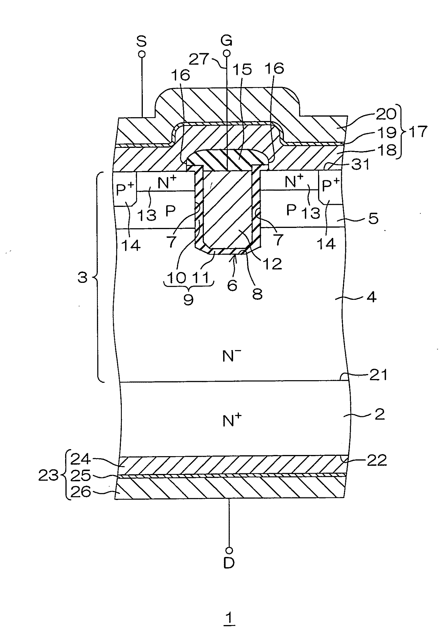
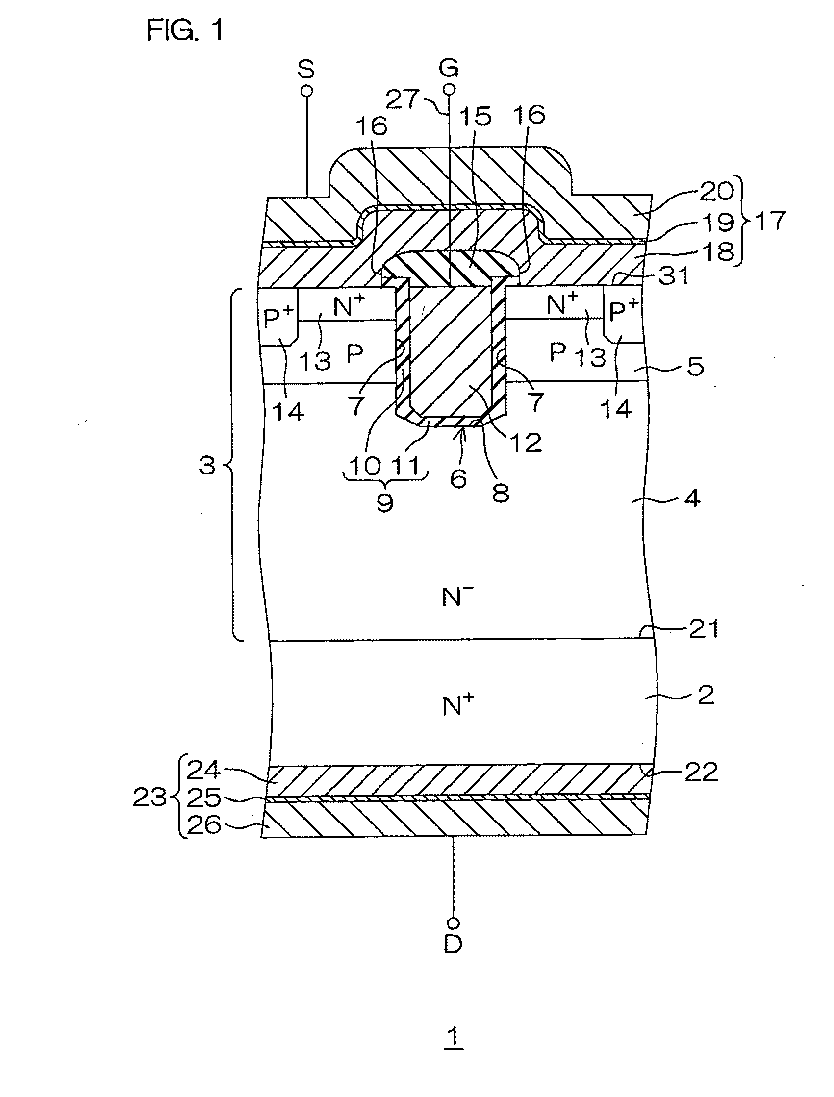
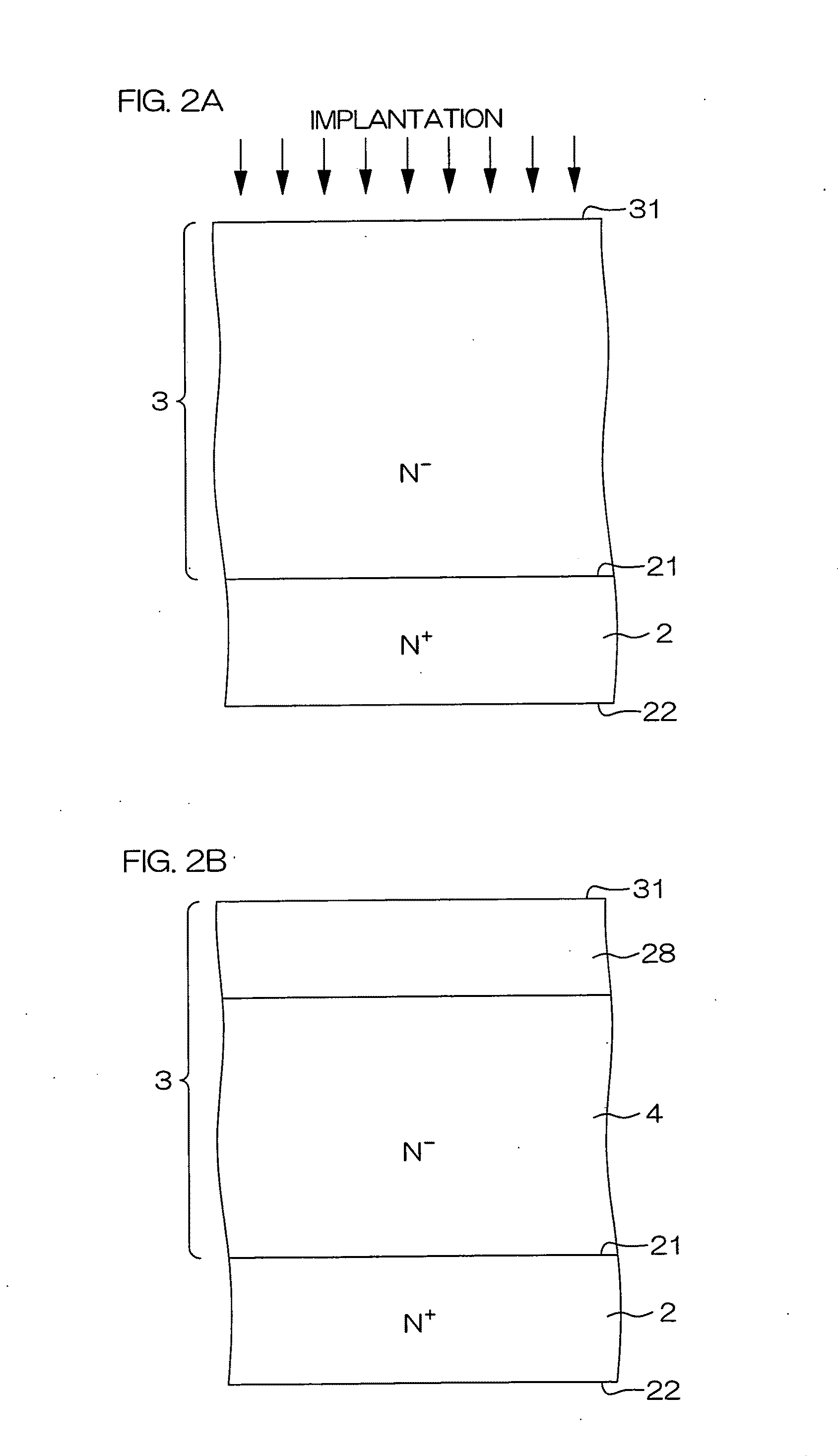
[0268]First, an epitaxial layer made of SiC was formed by growing an SiC crystal on an Si surface of a wafer-shaped SiC substrate (by Cree Inc.). Then, an N-type impurity was multistage-implanted from the surface (the Si surface) of the epitaxial layer with acceleration energy of 30 to 200 keV. Thus, an N-type impurity region (having a concentration of 1020 cm−3) was formed on a surface layer portion of the epitaxial layer.
[0269]Then, an insulating film made of SiO2 was formed on the surface of the epitaxial layer by CVD. Then, a contact hole was formed in the insulating film, to expose the aforementioned impurity region.
[0270]Then, a contact wire was obtained by forming a polysilicon layer by depositing a polysilicon material in the contact hole by CVD.
PUM
 Abstract
Description
Claims
Application Information