Light emitting semiconductor device and method of manufacture thereof

a technology of semiconductor devices and semiconductors, which is applied in the direction of semiconductor/solid-state device manufacturing, semiconductor devices, electrical devices, etc., can solve the problems of silver having the tendency to degrade easily, low light extraction efficiency, and high price of these devices, so as to reduce the risk of silver deformation, and improve the effect of light extraction efficiency

Active Publication Date: 2010-08-05
NICHIA CORP
View PDF4 Cites 144 Cited by
  • Summary
  • Abstract
  • Description
  • Claims
  • Application Information

AI Technical Summary

Benefits of technology

[0016]In this manner, leakage of light from the light emitting elements through the substrate can be suppressed to obtain a light emitting device with high light extraction efficiency. In particular, leakage of light from the light emitting elements through the substrate can be prevented, light reflective resin can be provided near the light emit

Problems solved by technology

Furthermore, supply of these devices at low prices while maximizing their performance is required.
However, silver has the tendency to degrade easily due to atmospheric constituents such as sulfur.
However, in the case of organic material covering silver, environmental resistance is problematic and the system can easily degra

Method used


Image

  • Light emitting semiconductor device and method of manufacture thereof
  • Light emitting semiconductor device and method of manufacture thereof
  • Light emitting semiconductor device and method of manufacture thereof

Examples


first embodiment

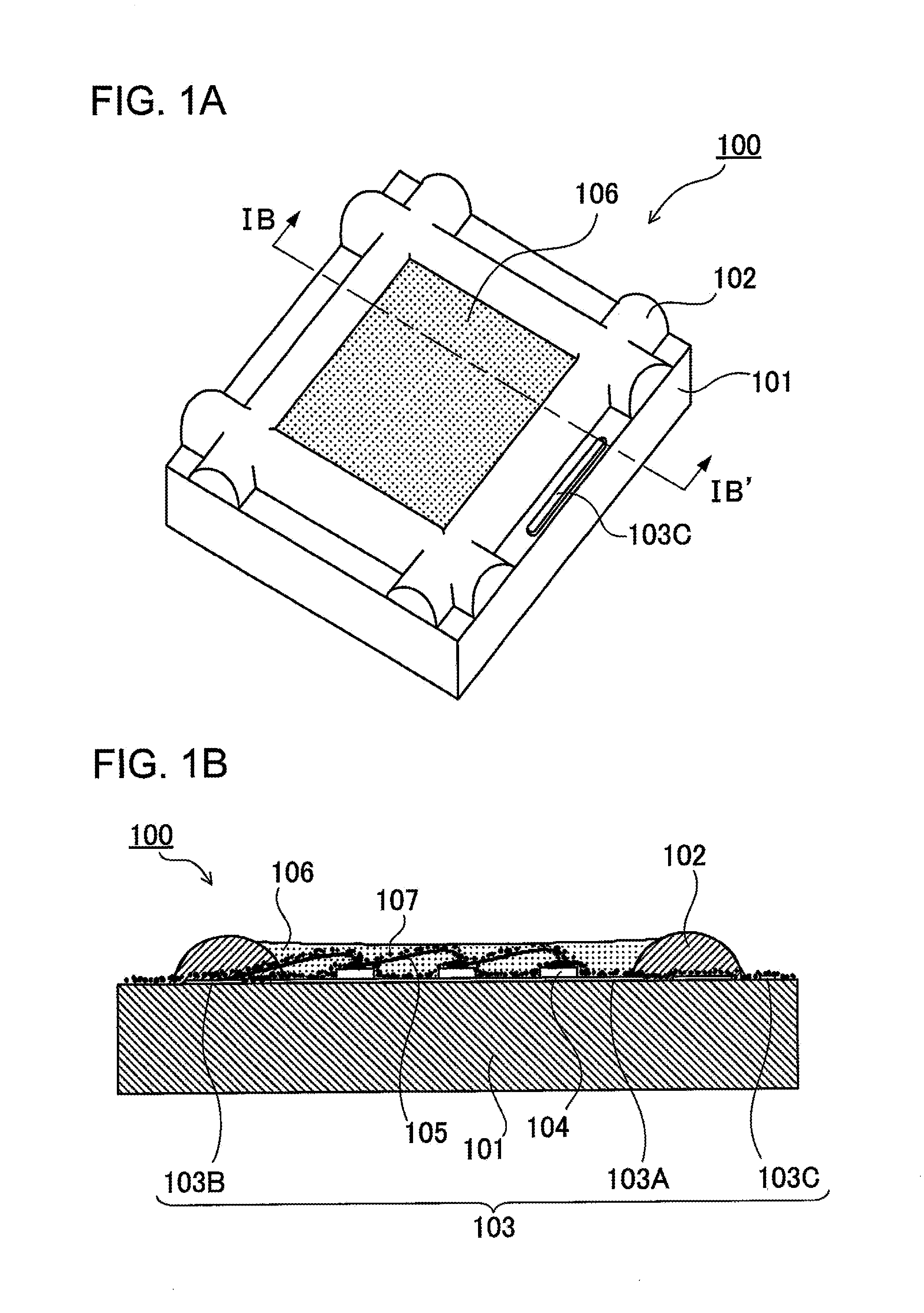
[0040]The following describes embodiments of the present invention based on the figures. First, FIGS. 1A and 1B show a light emitting device 100 for the first embodiment. FIG. 1A is an oblique view of the light emitting device 100, and FIG. 1B is a cross-section view through IB-IB′ on the light emitting device 100 shown in FIG. 1A. In this embodiment, the light emitting device 100 has an approximately rectangular substrate 101 with metallization 103A, 103B, 103C disposed on its upper surface, and a plurality of light emitting elements 104 mounted on the metallization 103A established on the upper surface of the substrate 101. Metallization 103A, 103B used as electrodes and the light emitting elements 104 are directly or indirectly connected electrically via conducting wire 105. Although metallization 103C is the same material as metallization 103A, 103B, which act as electrodes, it is not an electrically connected component, and is provided as a marker (cathode mark, anode mark) ind...

second embodiment

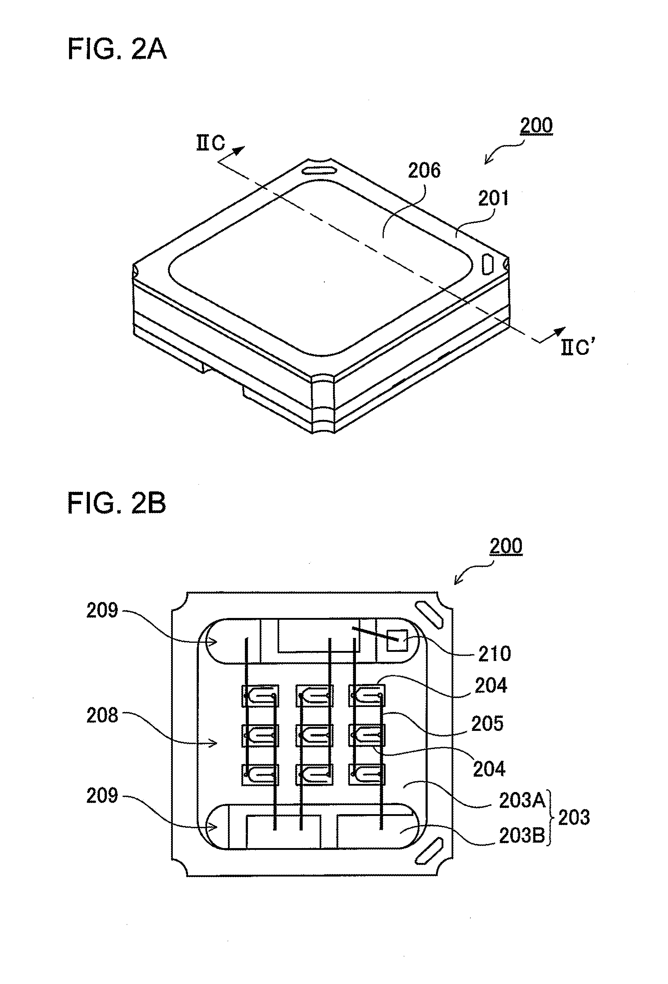
[0074]The light emitting device 200 of the second embodiment is shown in FIGS. 2A, 2B, and 2C. FIG. 2A is an oblique view of the light emitting device 200, FIG. 2B is a plan view of the light emitting device 200 shown in FIG. 2A looking through the encapsulating material 206, and FIG. 2C is a cross-section view through IIC-IIC′ on the light emitting device 200 shown in FIG. 2A. In the second embodiment, the light emitting device 200 has a substrate 201 provided with cavities having bottom and side surfaces, a plurality of light emitting elements 204 mounted on metallization 203A established on the bottom surface of a cavity, conducting wire 205 to electrically connect metallization 203B and light emitting elements 204, and encapsulating material 206 that covers components such as light emitting elements 204 and conducting wire 205. The cavities are a first cavity 208 in which the light emitting elements 204 are mounted, and second cavities 209 inside the first cavity 208 having bott...

third embodiment

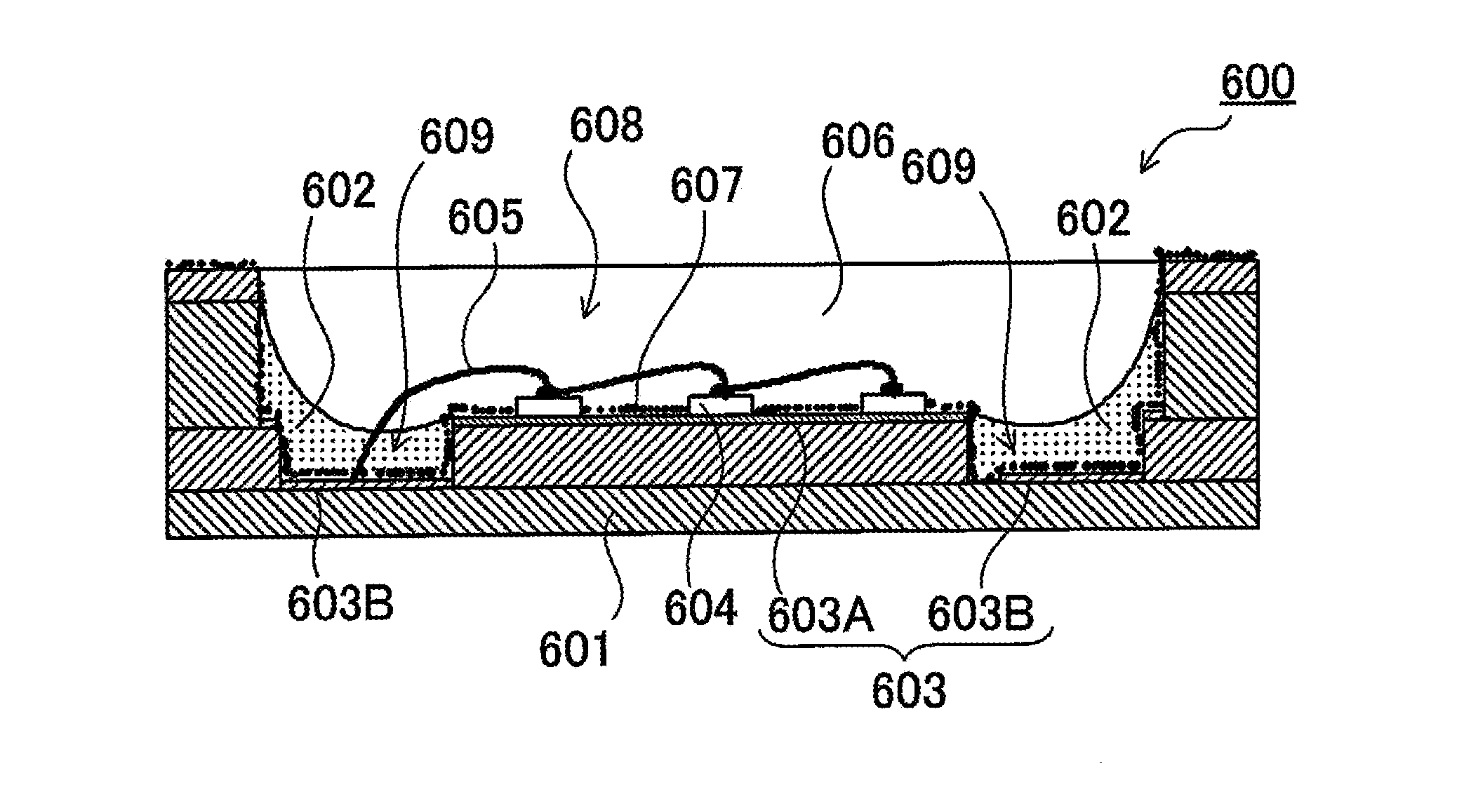
[0096]FIG. 3 shows a cross-section view of a light emitting device 300 for the third embodiment. The external appearance of the light emitting device 300 is similar in form to the light emitting device 100 shown in FIG. 1A, and the difference is the location where the insulating material 307 is formed. Specifically, the light emitting device of the third embodiment has a substrate 301 with metallization 303 (303A, 303B, 303C) that has metal including silver on its surface, light emitting elements 304 mounted on the substrate, conducting wire 305 that electrically connects metallization 303B and light emitting elements 304, encapsulating material 306 that fills the cavity surrounded by light reflective resin 302, light reflective resin 302 established on top of the substrate 301 to reflect light emitted by the light emitting elements 304, and insulating material 307 established on top of the light reflective resin 302. The insulating material 307 is established extending continuously...


PUM


Abstract

The light emitting device has a substrate, metallization including silver established on the surface of the substrate, a light emitting element mounted on the substrate, conducting wire that electrically connects the metallization and the light emitting element, light reflective resin provided on the substrate to reflect light from the light emitting element, and insulating material that covers at least part of the metallization surfaces. The insulating material is established to come in contact with the side of the light emitting element. This arrangement can suppress the leakage of light emitting element light from the substrate, and can achieve a light emitting device with high light extraction efficiency.

Description

BACKGROUND OF THE INVENTION[0001]1. Field of the Invention[0002]The present invention relates to a light emitting device that can be used in applications such as an indicator device, lighting equipment, display monitor, or backlight source for a liquid crystal display, and to the method of manufacturing the light emitting device. More particularly, the present invention relates to a light emitting device and its method of manufacture that has exceptional light extraction efficiency as well as high reliability.[0003]2. Description of the Related Art[0004]In recent years, various light emitting devices such as light emitting diode (LED) and laser diode (LD) apparatus that employ high output semiconductor light emitting elements (also referred to below simply as light emitting elements) have been developed.[0005]Recently, an assortment of electronic components have been proposed and developed, and demands on their performance has also increased. In particular, long-term, stable perform...

Claims


Application Information

Patent Timeline
IPC IPC(8): H01L33/00H01L21/50
CPCH01L25/0753H01L33/56H01L33/60H01L33/52H01L2224/45144H01L2224/48091H01L2224/48137H01L2224/48465H01L2224/8592H01L33/54H01L33/20H01L2924/01322H01L2924/00014H01L2924/00H01L2924/181H01L2924/00012H01L33/32H01L33/62H01L2933/005H01L2933/0058H01L2933/0066
Inventor INOBE, MOTOTAKAYAMADA, MOTOKAZUKAMADA, KAZUHIRO
Owner NICHIA CORP
Why Eureka
Try Eureka