Trench insulated gate bipolar transistor (GBT) with improved emitter-base contacts and metal schemes

a technology base contact, which is applied in the field of device configuration and manufacturing of insulated gate bipolar transistor, can solve the problems of increase collector-emitter saturation voltage, and high gate-emitter threshold voltage, so as to enhance the latch-up immunity capability of the igbt device, reduce the base contact resistance

Inactive Publication Date: 2010-08-05
FORCE MOS TECH CO LTD
View PDF3 Cites 41 Cited by
  • Summary
  • Abstract
  • Description
  • Claims
  • Application Information

AI Technical Summary

Benefits of technology

[0009]It is therefore an aspect of the present invention to provide a new and improved insulation gate bipolar transistor (IGBT) power device by forming emitter-base contact dopant regions underneath an emitter-dopant contact trenches. The emitter-base contact dopant regions are formed at a distance away from the channels near the trench gate. The emitter-base dopant contact regions reduce the base contact resistance. The emitter-base contact dopant regions are further formed at a distance away from the channel regions. The emitter-base contact dopant regions can therefore enhance latch-up immunity capability of the IGBT device without increase the gate-emitter threshold voltage.

Problems solved by technology

However, conventional high voltage semiconductor power devices such as the insulated gate bipolar transistor (IGBT) devices are still confronted with the technical difficulties caused by an increased collector-emitter saturation voltage.
However, the device as shown in FIG. 1A has a disadvantage that the P+base 51 touches the channel region thus causes a high gate-emitter threshold voltage that in turn increases the collector-emitter saturation voltage.
The IGBT disclosed by Huang has a disadvantage due to the P+ base region 35 deeper than the base region 14 thus causing a high JFET resistance between two adjacent contact trenches.

Method used


Image

  • Trench insulated gate bipolar transistor (GBT) with improved emitter-base contacts and metal schemes
  • Trench insulated gate bipolar transistor (GBT) with improved emitter-base contacts and metal schemes
  • Trench insulated gate bipolar transistor (GBT) with improved emitter-base contacts and metal schemes

Examples


Embodiment Construction

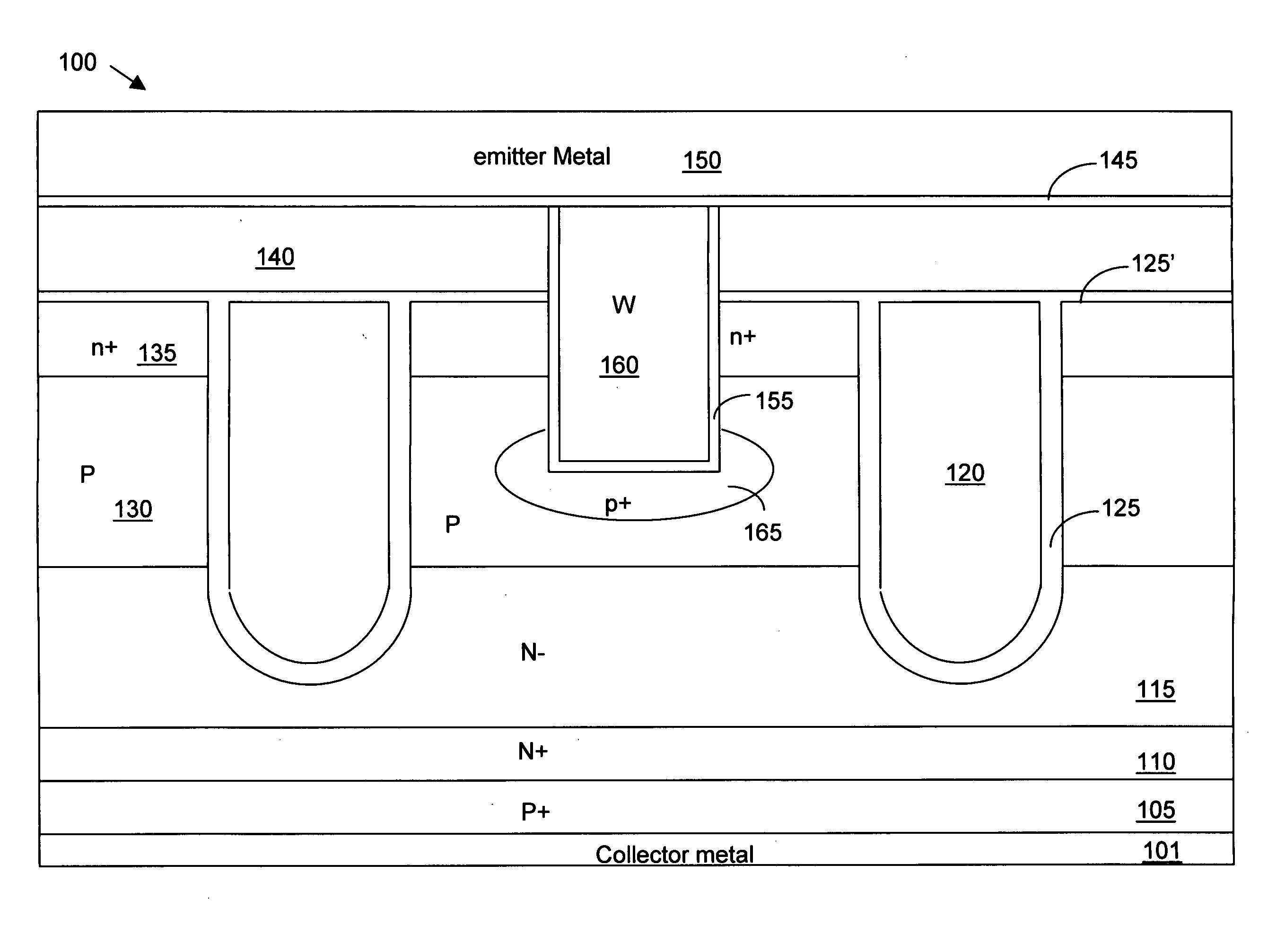
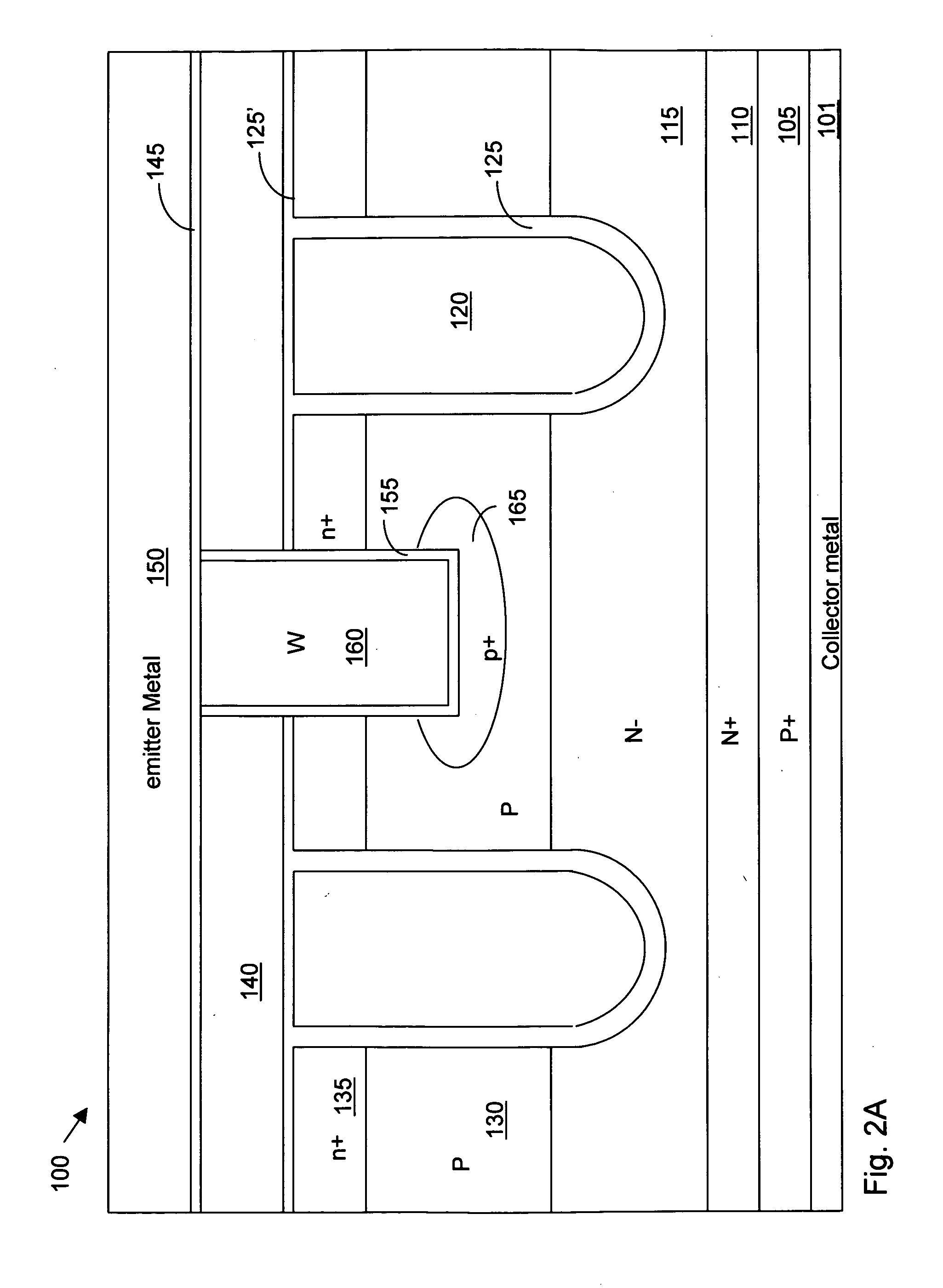
[0017]Referring to FIG. 2A for a side cross sectional view of an insulated gate bipolar transistor (IGBT) device 100 formed as a vertical power device on a P+ semiconductor substrate 105. The IGBT device is a punch-through (PT) type of IGBT device. The P+ substrate 105 functions as a collector region with a collector metal 101 formed on the bottom surface. The P+ substrate 105 supports N+ and N− epitaxial layers 110 and 115 grown on top of the P+ substrate 105 for functioning as a buffer layer and N-base layer respectively. The IGBT device further comprises trench gates 120 filled with gate dielectric layer such as polysilicon and padded with gate oxide layer 125. The trench gates are surrounded by P-base regions 130 that encompass N+ emitter regions 135 formed near the top surface of the substrate. The top surface of the substrate is covered with an insulation layer 140 on overlaying the insulation layer 125′ formed together with the gate insulation layer 125.

[0018]The IGBT device ...


PUM


Abstract

A trench insulation gate bipolar transistor (IGBT) power device includes a plurality of trench gates surrounded by emitter regions of a first conductivity type near a top surface of a semiconductor substrate encompassed in base regions of a second conductivity type and a collector layer disposed at a bottom surface of the semiconductor substrate. The trench IGBT power device further includes an insulation layer covering over the top surface over the trench gate and the emitter regions having emitter-base contact trenches opened therethrough between the trench gates and extending to the base regions and an emitter-base contact dopant region disposed in the base region of the second conductivity type surrounding a lower region of the contact trenches. The emitter-base contact dopant region is disposed at a distance away from a channel near the trench gates for reducing an emitter-base resistance without increasing a gate-emitter threshold voltage.

Description

BACKGROUND OF THE INVENTION[0001]1. Field of the Invention[0002]The invention relates generally to a device configuration and method of manufacturing an insulated gate bipolar transistor (IGBT). More particularly, this invention relates to an improved IGBT device configuration and manufacturing method for a trench IGBT that has improved emitter-base contacts and metal schemes.[0003]2. Description of the Relevant Art[0004]As a key component in the power electronic systems, the semiconductor power devices are commonly implemented in the power electronic systems such as the power systems for the hybrid, electric or fuel cells vehicles. Recently, there are increasing demands for high performance semiconductor power devices. Particularly, there are increasing demands for high performance high voltage semiconductor power devices such as the insulated gate bipolar transistor (IGBT) devices. However, conventional high voltage semiconductor power devices such as the insulated gate bipolar tr...

Claims


Application Information

Patent Timeline
Patent Type & Authority Applications(United States)
IPC IPC(8): H01L29/739H01L21/331
CPCH01L29/41708H01L29/7397H01L29/66348
Inventor HSHIEH, FWU-IUAN
Owner FORCE MOS TECH CO LTD
Why Eureka
Try Eureka