Semiconductor device and electric power conversion device using same

A semiconductor and conductive technology, which is applied in the direction of semiconductor devices, circuits, transistors, etc., can solve the problems of IGBT withstand voltage drop, and achieve the effects of suppressing overcurrent, low noise, and high damage resistance

Inactive Publication Date: 2012-10-03
HITACHI LTD
View PDF11 Cites 4 Cited by
  • Summary
  • Abstract
  • Description
  • Claims
  • Application Information

AI Technical Summary

Problems solved by technology

[0020] As mentioned above, in the conventional IGBT, the current flows only in the part where the distance between the tunnel gates is narrow, and the floating p layer is provided to suppress the flow of overcurrent in the event of a short circuit, but there is noise (potential Displacement, current vibration), if the distance between the tunnel gate and the floating p-layer is widened in order to avoid these noises, there will be a concentration of the electric field at the corner of the tunnel gate (including the gate insulating film), resulting in a drop in the withstand voltage of the IGBT The problem

Method used


Image

  • Semiconductor device and electric power conversion device using same
  • Semiconductor device and electric power conversion device using same
  • Semiconductor device and electric power conversion device using same

Examples


no. 1 approach

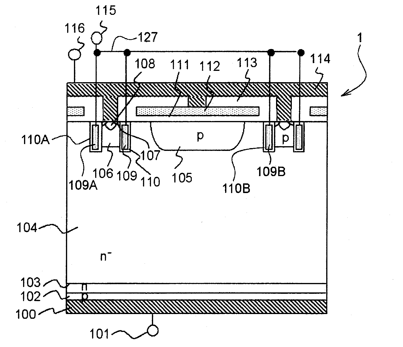
[0043] figure 1 It is a cross-sectional view showing the structure of tunnel gate IGBT1 which is the first embodiment of the semiconductor device of the present invention. figure 1 A form in which IGBTs are formed on a silicon substrate (semiconductor substrate) is shown. The silicon substrate is in the shape of a thin wafer, and each element structure constituting the IGBT is formed on the front surface and the back surface (a pair of surfaces).

[0044] exist figure 1 Among them, the structure that performs the basic operation as IGBT1 is p collector layer (first semiconductor layer) 102, n buffer layer (second semiconductor layer) 103, n - Drift layer (third semiconductor layer) 104 , p channel layer (fourth semiconductor layer) 106 , gate electrode 109 , n emitter layer (fifth semiconductor layer) 107 . It should be noted that, since the gate electrode 109 is provided in a deep-dug vertical hole as a tunnel structure, it may be shown as a tunnel gate 109 .

[0045] In...

no. 4 approach

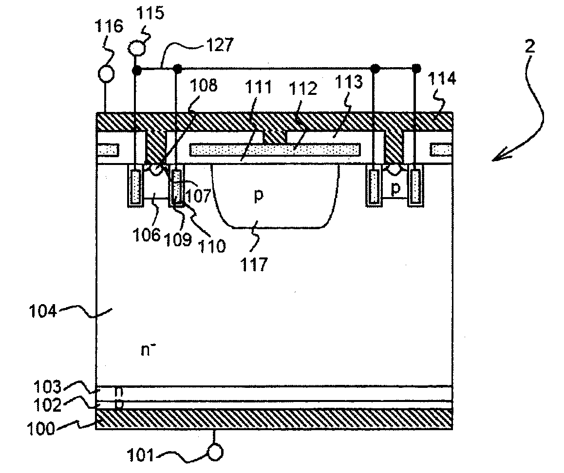
[0083] Figure 7 It is a cross-sectional view showing the structure of a tunnel gate type IGBT 4 which is a fourth embodiment of the semiconductor device of the present invention.

[0084] exist Figure 7 Among them, as the basic operation structure of IGBT4, p collector layer 102, n buffer layer 103, n - Drift layer 104 , p channel layer 106 , gate electrode 109 , n emitter layer 107 .

[0085] In addition, in order to use them as elements of the practical IGBT4, the collector electrode 100, the collector terminal 101, the emitter electrode 114, the emitter terminal 116, the gate wiring electrode 127, the gate terminal 115, and the gate insulating film are provided. 110 , p-contact layer 108 , and insulating film 113 .

[0086] In addition, in order to ensure noise reduction and withstand voltage, floating p-layer 105 , insulating film 111 , and polycrystalline silicon 112 are provided.

[0087] above, due to the figure 1 The structure of the structure is substantially ...

no. 6 approach

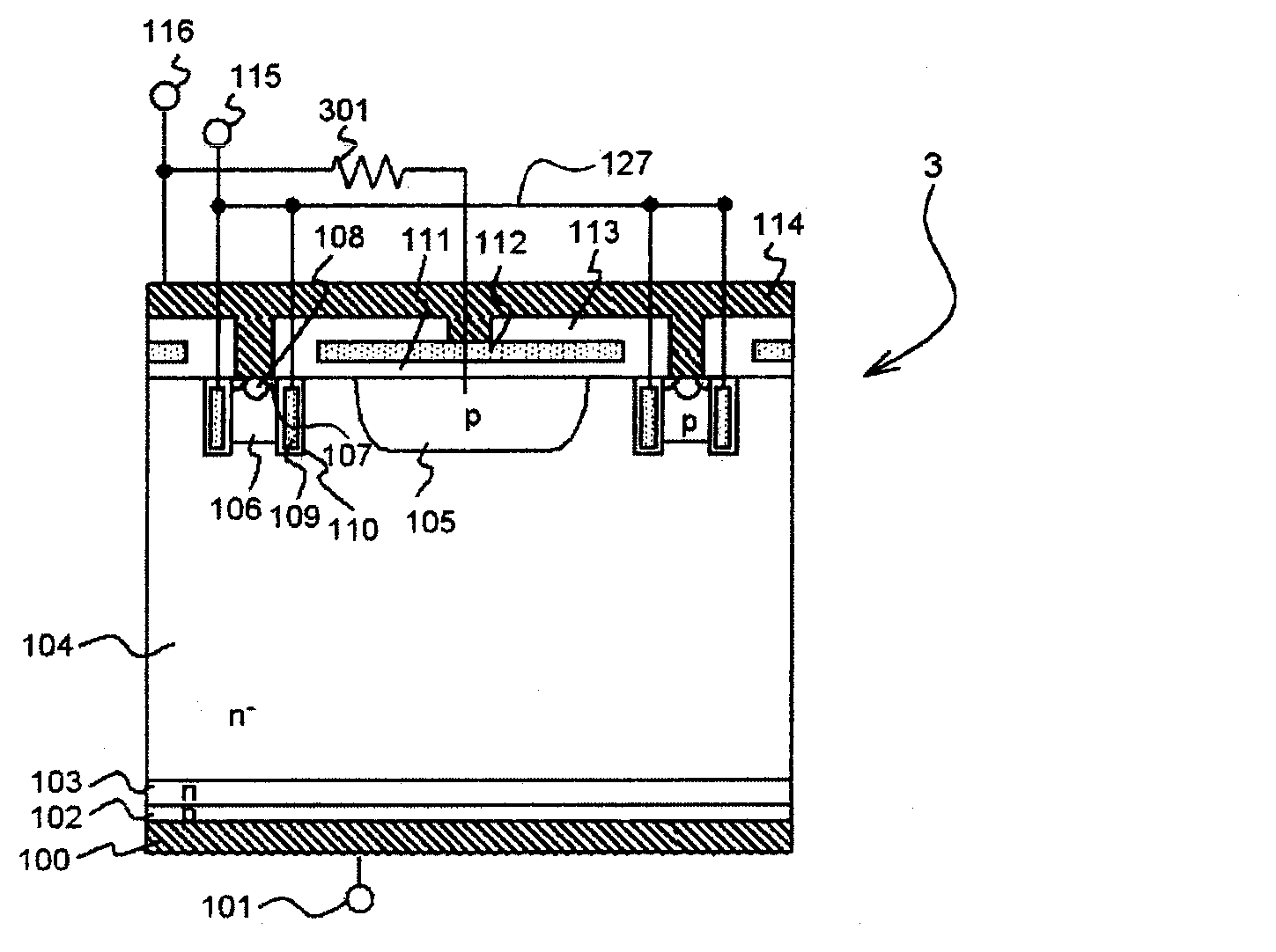
[0101] Figure 9 It is a cross-sectional view showing the structure of a tunnel gate type IGBT 6 which is a sixth embodiment of the semiconductor device of the present invention.

[0102] exist Figure 9 In, as the p collector layer 120 of IGBT6, n buffer layer 121 and figure 1 Unlike the first embodiment, the n-emitting layer 107 ( 107B, 107C) is formed on the same surface side of the silicon substrate. The structure of this embodiment is characterized in that the structure of Embodiment 1 of the vertical structure is reconfigured as a horizontal structure.

[0103] The structure that performs the basic operation as IGBT6 is p collector layer 120, n buffer layer 121, n drift layer 104, p channel layer 106 (106B), gate electrode 109 (109B, 109C), n emitter layer 107 (107B, 107C).

[0104] Tunnel gate type IGBT 6 supplies a positive polarity power supply potential to p collector layer 102 , and further performs ON / OFF control using the potential supplied to gate electrode ...


PUM


Abstract

The invention provides a semiconductor device and an electric power conversion device using same. Specifically, disclosed is an IGBT that suppresses overcurrent flowing during a short-circuit, while being low-loss and low-noise (low electric potential displacement, low current oscillation), and wherein an element has high fracture tolerance. The IGBT is a trench IGBT; is provided with a plurality of trench gates disposed in a manner so as to form two types (wide and narrow) of gaps; has a MOS structure that has a channel of a first conductivity type and that is between the aforementioned trench gate pair that is disposed with a narrow gap therebetween; and is provided with a floating semiconductor layer of the first conductivity type and that is separated from the aforementioned trench gates by interposing a portion of a third semiconductor layer of a second conductivity type between the aforementioned trench gate pair that is disposed with a wide gap therebetween. Also, this floating semiconductor layer is disposed parallel to and at a position corresponding to an emitter electrode and a first semiconductor layer having the same electric potential, with a insulating film therebetween. By means of the above structure, the electric field concentration in the corner sections of the aforementioned trench gates is eased, voltage resistance is increased, and low noise and low loss are achieved.

Description

technical field [0001] The present invention relates to a structure of an insulated gate bipolar transistor (IGBT: Insulated Gate Bipolar Transistor; hereinafter abbreviated as IGBT) and a power conversion device using the IGBT. Background technique [0002] An IGBT is a switching element that controls the current flowing between a collector electrode and an emitter electrode by applying a voltage to a gate electrode. Because the power that IGBT can control ranges from tens of watts to hundreds of thousands of watts, and the switching frequency ranges from tens of hertz to more than hundreds of kilohertz, it is widely used in low-power equipment such as household air conditioners and electronic microwave ovens to railways. , Inverters in ironworks and other high-power equipment are widely used. [0003] IGBTs are required to reduce their losses in order to achieve higher efficiency of these power devices, and thus reductions in conduction losses and switching losses are req...

Claims


Application Information

Patent Timeline
Patent Type & Authority Applications(China)
IPC IPC(8): H01L29/739H01L27/04H01L29/78H01L29/786
CPCH01L29/7397H01L29/402H01L27/0664H01L29/0619H01L29/0839H01L29/1095
Inventor 白石正树森睦宏铃木弘渡边聪
Owner HITACHI LTD
Why Eureka
Try Eureka