Method for reclaiming a surface of a substrate

a technology of a substrate and a surface is applied in the field of reclaiming a substrate surface, which can solve the problems of inability to meet the requirements of reclaiming, the surface is easily recycled, and the desired structure cannot be quickly achieved, so as to improve the quality of the reclaimed substrate, the effect of rapid reclaiming

Inactive Publication Date: 2010-08-12
S O I TEC SILICON ON INSULATOR THECHNOLOGIES
View PDF2 Cites 14 Cited by
  • Summary
  • Abstract
  • Description
  • Claims
  • Application Information

AI Technical Summary

Benefits of technology

[0024]According to an exemplary embodiment, the method can further comprise an edge polishing step to remove an ion implanted region in the chamfered edge area of the substrate. This additional step helps to further improve the quality of the reclaimed substrate.
[0025]A substrate which comprises a base, an ion implanted region as well as a non-ion implanted region over the base, in particular in a edge region of the base, a first layer of a first material on the ion implanted region, an

Problems solved by technology

Even though it is possible to obtain a recycled substrate that can be reused in the Smart Cut™ process using the reclaiming process described above, this process includes a double-sided polishi

Method used


Image

  • Method for reclaiming a surface of a substrate
  • Method for reclaiming a surface of a substrate
  • Method for reclaiming a surface of a substrate

Examples


first embodiment

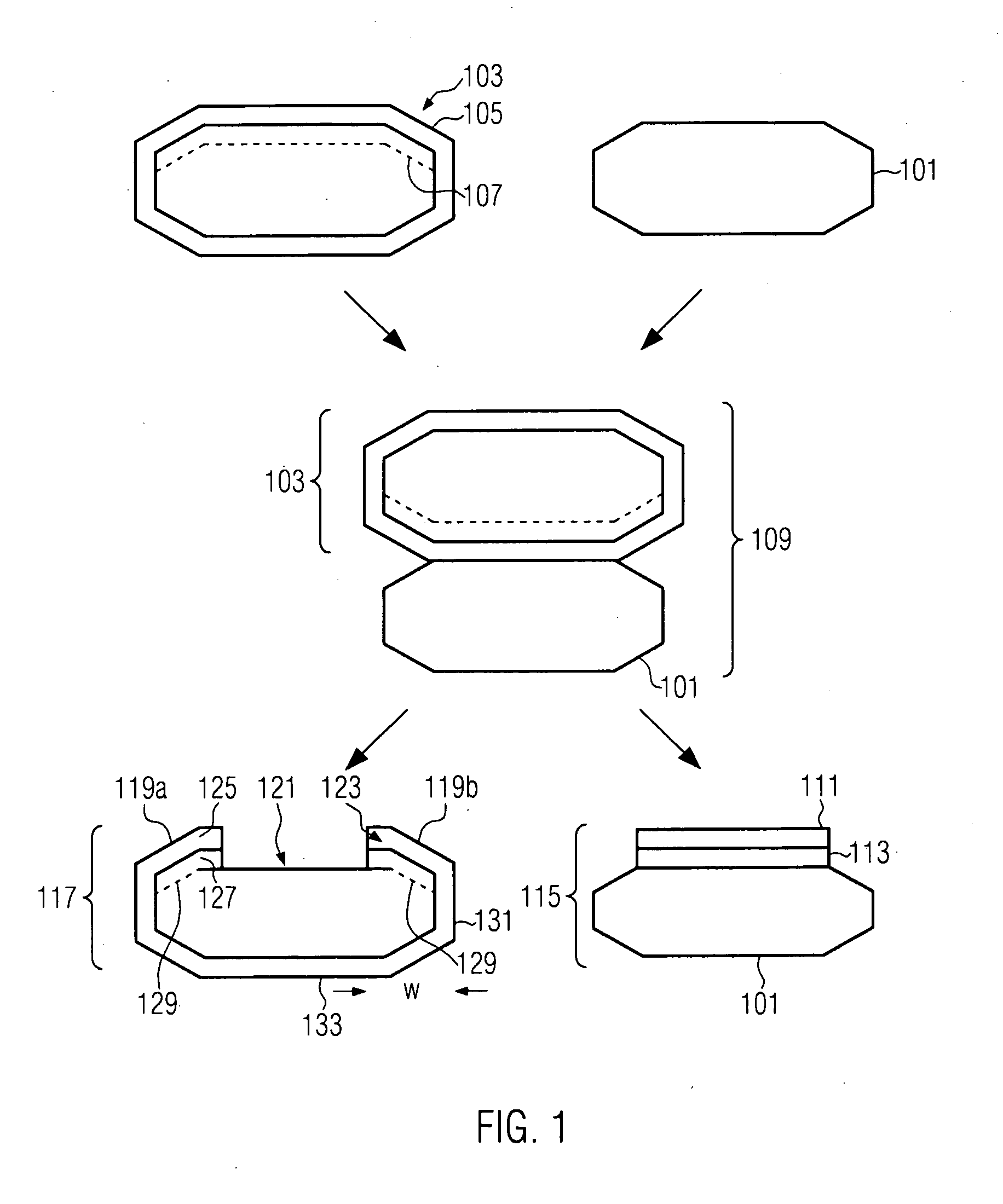
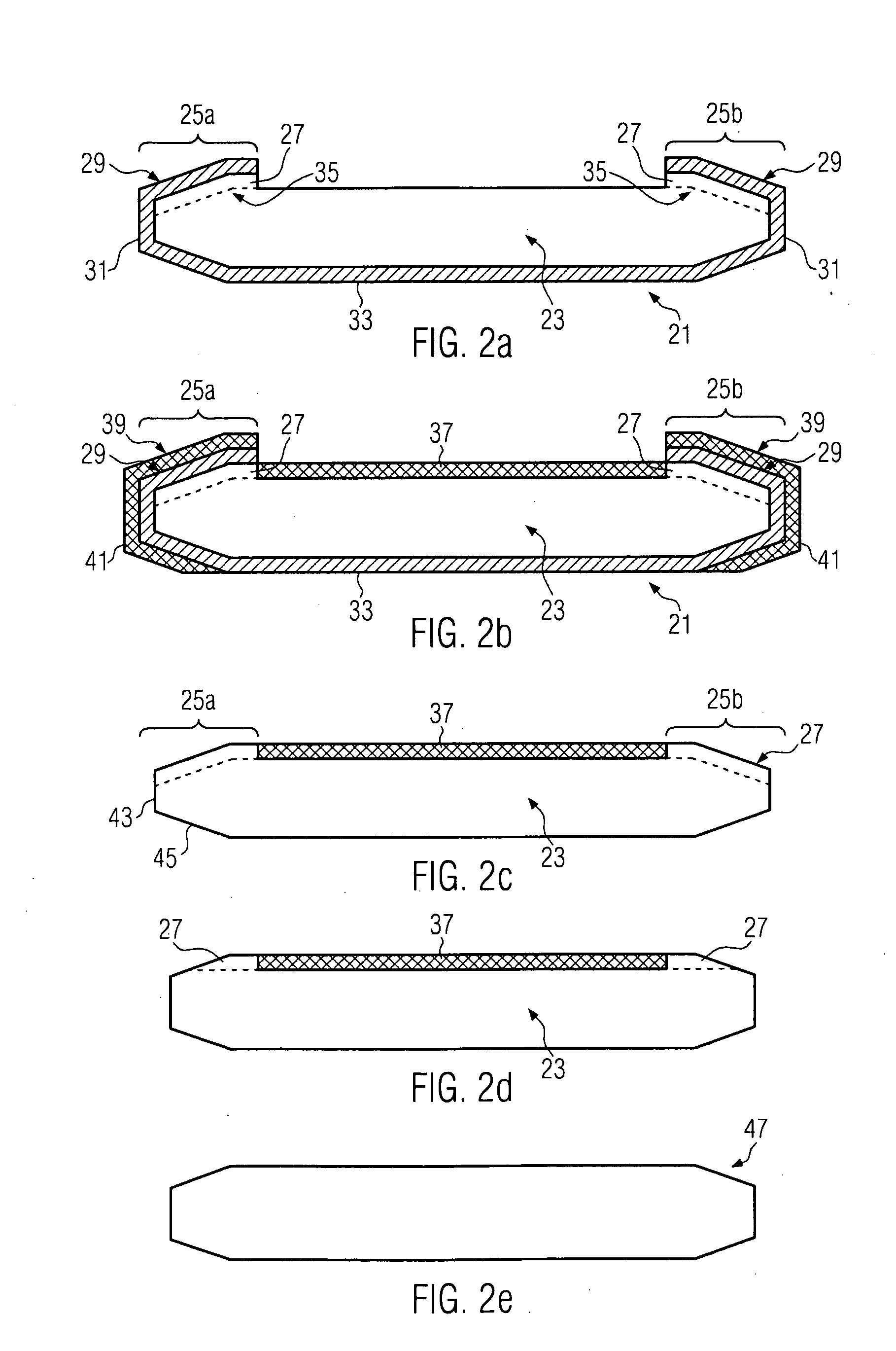
[0032]For purposes of illustration, and not limitation, FIGS. 2a-2e illustrate the invention, wherein the oxide layer of the remainder is used as a physical mask. FIG. 2a illustrates schematically a remainder 21 of a donor substrate which has been used in a layer transfer process like, for example, the Smart Cut™ process described above in relation to FIG. 1. The remainder 21 illustrated in FIG. 2a corresponds to the negative 117 illustrated in FIG. 1.

[0033]The reminder 21 comprises a base layer 23,which may be made of, for example, silicon or germanium. The surface in the edge region of the base layer 23 carries a protruding topography 25a and 25b. As was the case with the structure shown in FIG. 1, this protruding residual topography 25a, 25b is the result of non-transferred parts due to the edge geometry of the wafers comprising a chamfered region. The protruding topography in this embodiment comprises a step-like residual first layer 27, such as silicon or germanium, and a secon...

second embodiment

[0046]FIGS. 3a-3e illustrate the method for reclaiming a surface of a substrate, wherein the surface, in particular a silicon surface, comprises a protruding residual topography. FIG. 3a again illustrates the substrate 21 to be reclaimed, as illustrated in FIG. 2a, as well as FIG. 1. The description of substrate 21 and its elements will thus not be repeated again in detail, but reference is made to the description of FIG. 2a.

[0047]The difference between the first and second embodiments is that the filling material is deposited using a different kind of process. Whereas in the first embodiment a process was chosen during which the filling material 37 was present over the entire substrate 21 except the backside 33, the second embodiment proposes a process wherein the second layer 29, thus the oxide layer, plays a different role. In the second embodiment, the oxide layer 29 is a chemical mask so that during deposition of a filling material 51, again polycrystalline silicon, the deposi...


PUM

PropertyMeasurementUnit
Fractionaaaaaaaaaa
Fractionaaaaaaaaaa
Fractionaaaaaaaaaa

Abstract

A method for reclaiming a surface of a substrate, wherein the surface, in particular a silicon surface, comprises a protruding residual topography, comprising at least the layer of a first material. By providing a filling material in the non-protruding areas of the surface of the substrate and the subsequent polishing, the reclaiming can be carried out such that the material consuming double-sided polishing step used in the prior art is no longer necessary.

Description

CROSS REFERENCE TO RELATED APPLICATION[0001]This application claims priority to European Patent Application No. EP09290104, filed Feb. 12, 2009, which is incorporated herein by reference in its entirety.BACKGROUND[0002]1. Field of the Disclosure[0003]The present disclosure relates to a method for reclaiming a surface of a substrate. In particular, the present disclosure relates to a method for reclaiming a surface of a silicon substrate that includes a protruding residual topography resulting from a layer transfer process typically comprising an ion implantation step, a bonding step and a detachment step.[0004]2. Description of Related Art[0005]The so-called Smart Cut™ process, illustrated in FIG. 1, provides high quality silicon on insulator (SOI) substrates. During this process, two substrates, called a handle substrate 101 and a donor substrate 103, usually a silicon wafer, undergo a certain number of process steps to transfer a layer with a given thickness of the donor substrate...

Claims


Application Information

Patent Timeline
IPC IPC(8): H01L29/04H01L21/20H01L29/02
CPCH01L21/02032H01L21/76254H01L21/304H01L21/02H01L27/12
Inventor ALAMI-IDRISSI, AZIZKERDILES, SEBASTIENSCHWARZENBACH, WALTER
Owner S O I TEC SILICON ON INSULATOR THECHNOLOGIES
Why Eureka
Try Eureka