

Light emitting element and light emitting device using the light emitting element
- Summary
- Abstract
- Description
- Claims
- Application Information
AI Technical Summary
Benefits of technology
Problems solved by technology
Method used
Image

Examples
embodiments
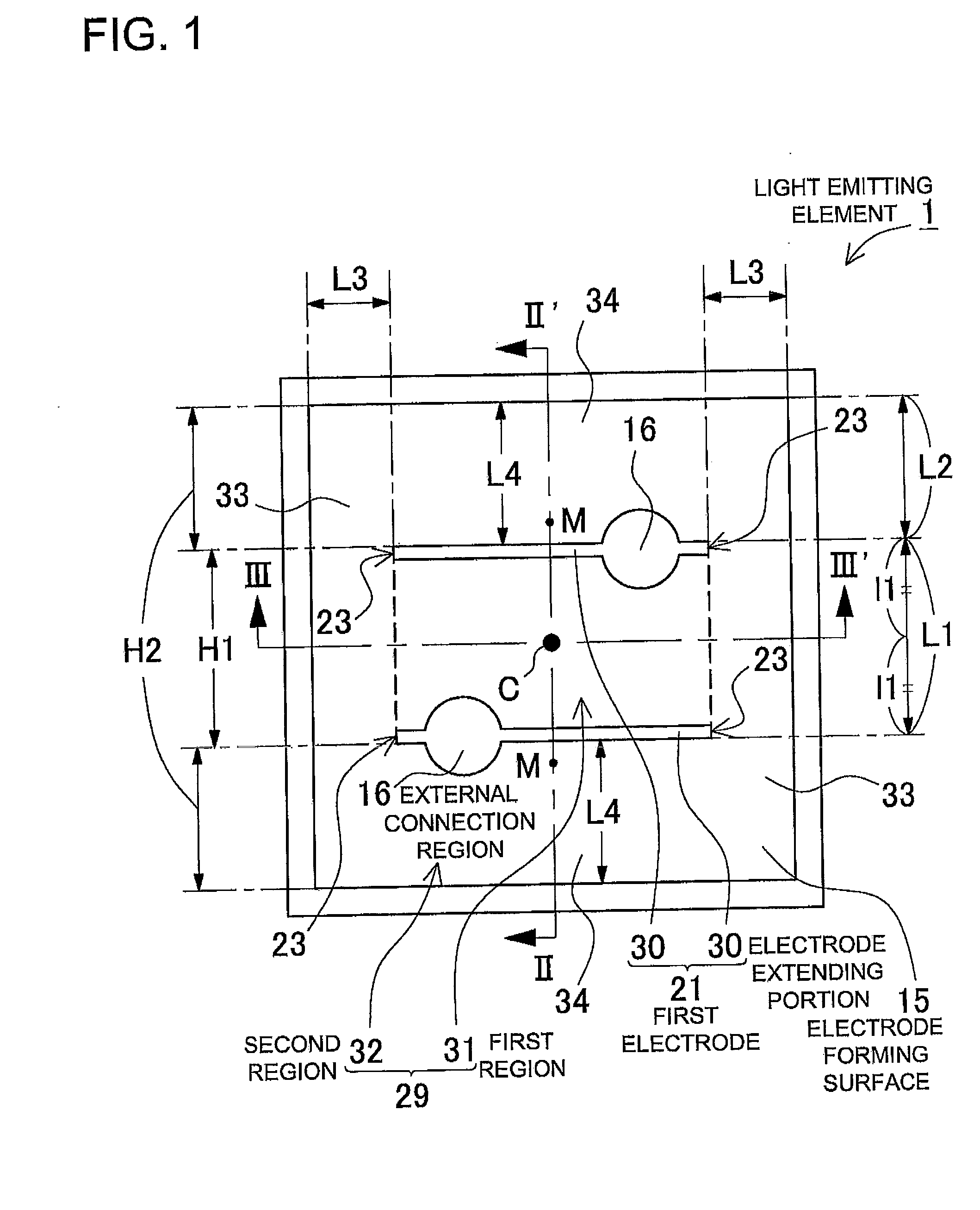
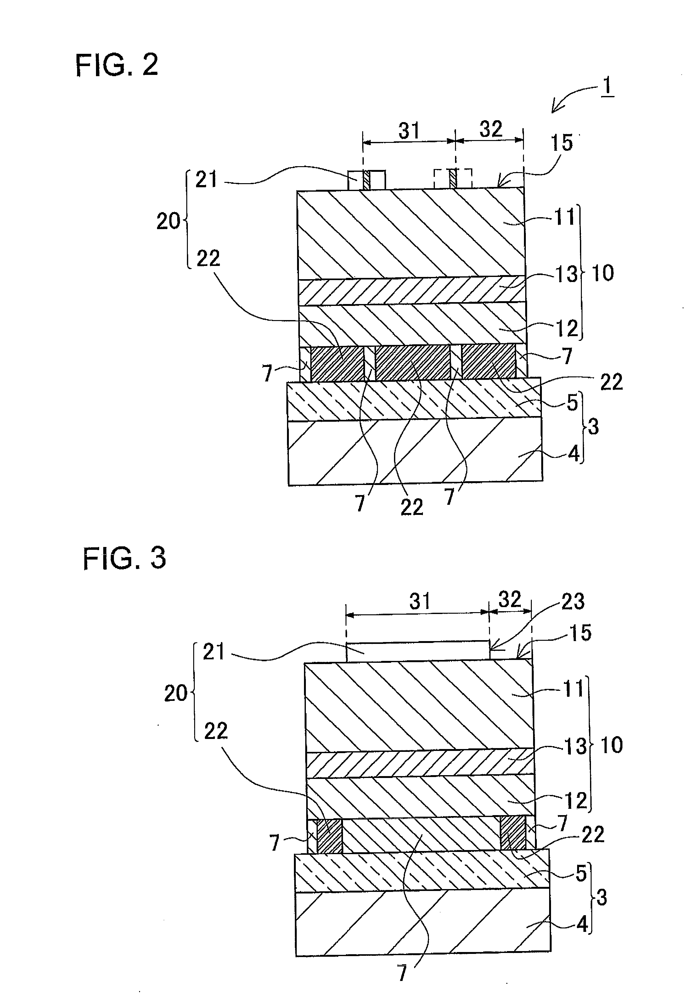
[0042]A plan view shown in FIG. 1 is an example of a light emitting element 1 according to the present embodiment. FIG. 2 is a cross sectional view taken along line II-II′ of FIG. 1, and FIG. 3 is a cross sectional view taken along line III-III′ of FIG. 1, respectively.
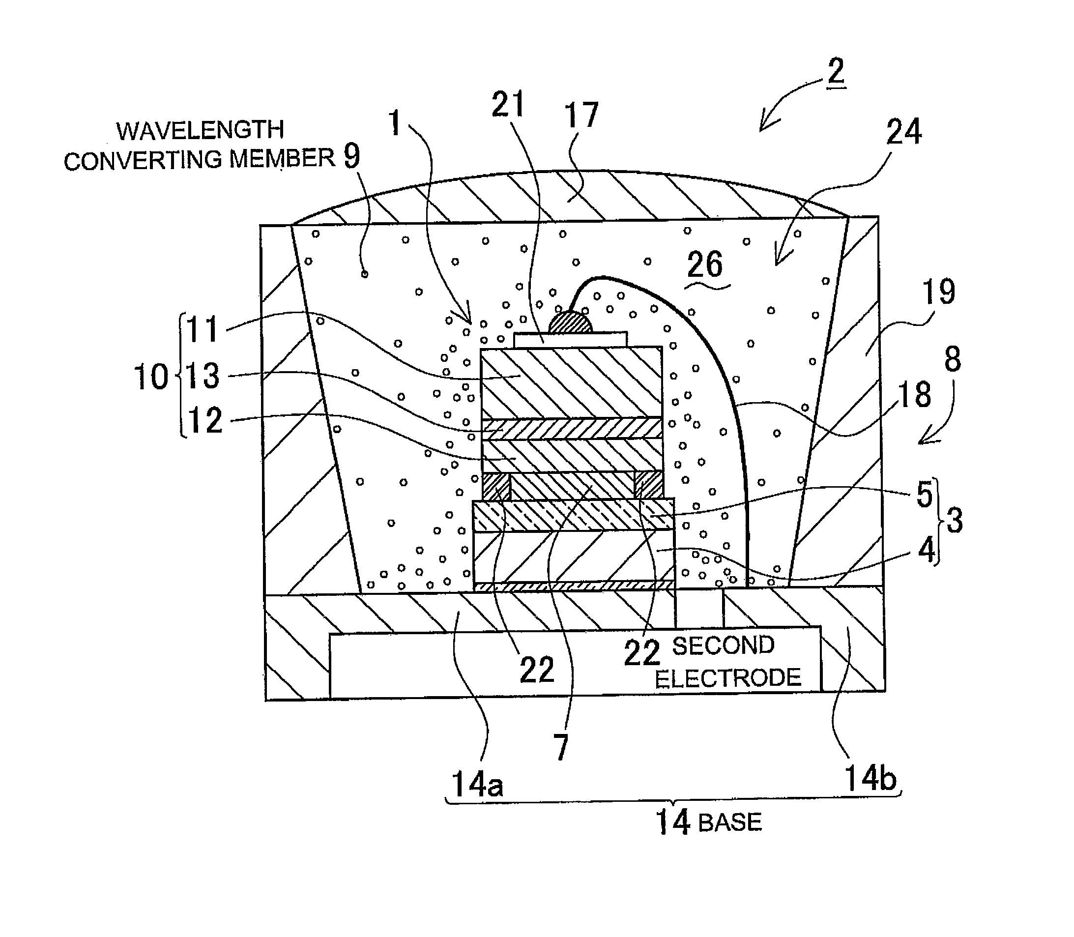
[0043]The light emitting element 1 shown in FIG. 2 or FIG. 3 is mainly constructed of a support pedestal 3, a semiconductor structure 10 positioned above the support pedestal 3, an electrode portion 20 interposing upper and lower surfaces of the semiconductor structure 10. Also, the support pedestal 3 is fixed by a support substrate 4 and a bonding layer 5 stacked in this order. The semiconductor structure 10 includes a light emitting layer 13, a n-type semiconductor layer which is a first conductive type layer 11 stacked interposing the light emitting layer 13, and a p-type semiconductor layer which is a second conductive type layer 12. In the example shown in the figures, the p-type semiconductor layer 12, the light...
example 1
[0114]A configuration of an electrode according to Example 1 will be shown below. Herein, members of the same quality as described above are assigned the same reference numerals and detailed description thereof will be omitted. FIG. 10 is a plan view of a light emitting element 101 seen from its light extracting side, and is mainly illustrating an n-electrode 41. The light emitting element 101 shown in FIG. 10 is a dice having an substantially square shape of 1 mm (electrode forming surface of 1 mm×1 mm). The circumferential shape thereof is formed by a first end 35 extending in one direction (the right and left direction in FIG. 10), a second end 36 perpendicular to the first end, and two ends 35′, 36′ positioned respectively opposite to and in parallel with the two ends 35, 36.
[0115]The n-electrode 41 has a pair of electrode pad portions 16 formed in the electrode forming surface 15 which is an exposed portion of the n-type semiconductor layer 11, and an electrode extending porti...
example 2
[0125]A light emitting element having a structure as that of the light emitting element of Example 1 is provided with the electrodes whose shape and arrangement are made in a scaled-down manner. With this light emitting element of 800 μm, good optical output and heat dissipation can be obtained as in Example 1.
PUM
 Abstract
Description
Claims
Application Information