

Laser soldering apparatus
a technology of laser soldering and soldering rod, which is applied in the direction of soldering apparatus, manufacturing tools, printed circuit manufacturing, etc., can solve the problems of low productivity and inability to observe the base end of the lead portion of the component through the hole, and achieve high speed and quality. high
- Summary
- Abstract
- Description
- Claims
- Application Information
AI Technical Summary
Benefits of technology
Problems solved by technology
Method used
Image

Examples
first embodiment
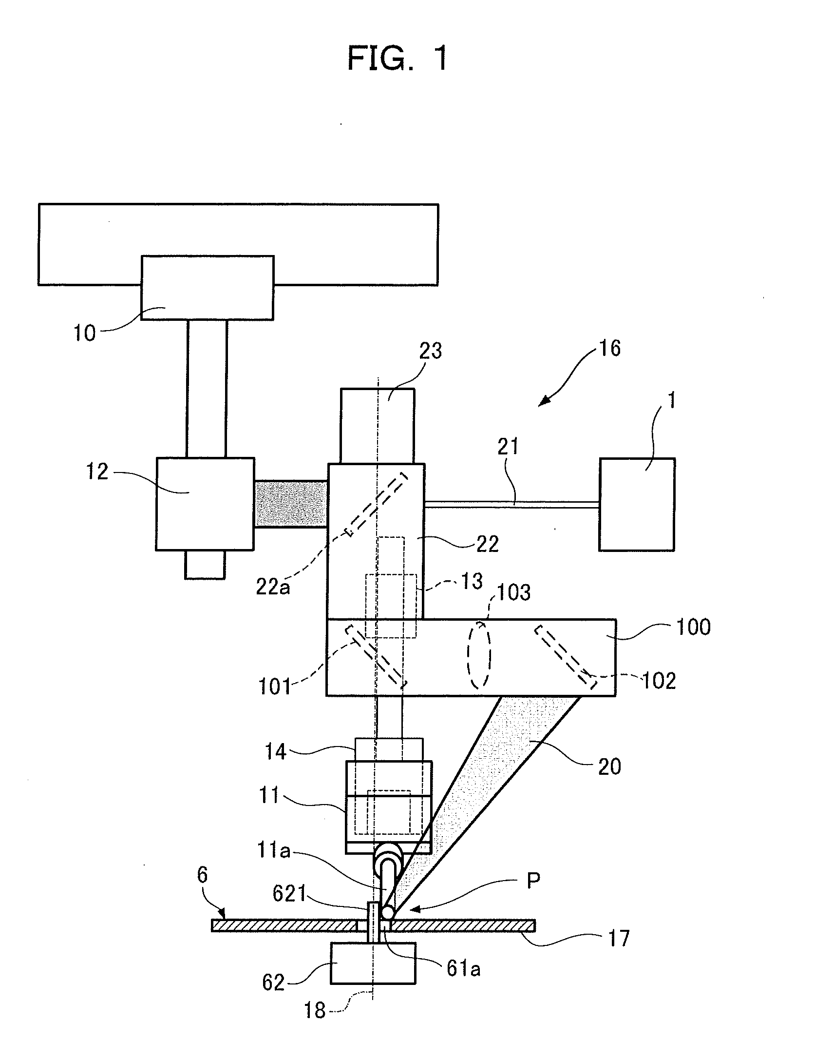
[0043]FIG. 1 to FIGS. 5A and 5B show a first embodiment of the present invention.
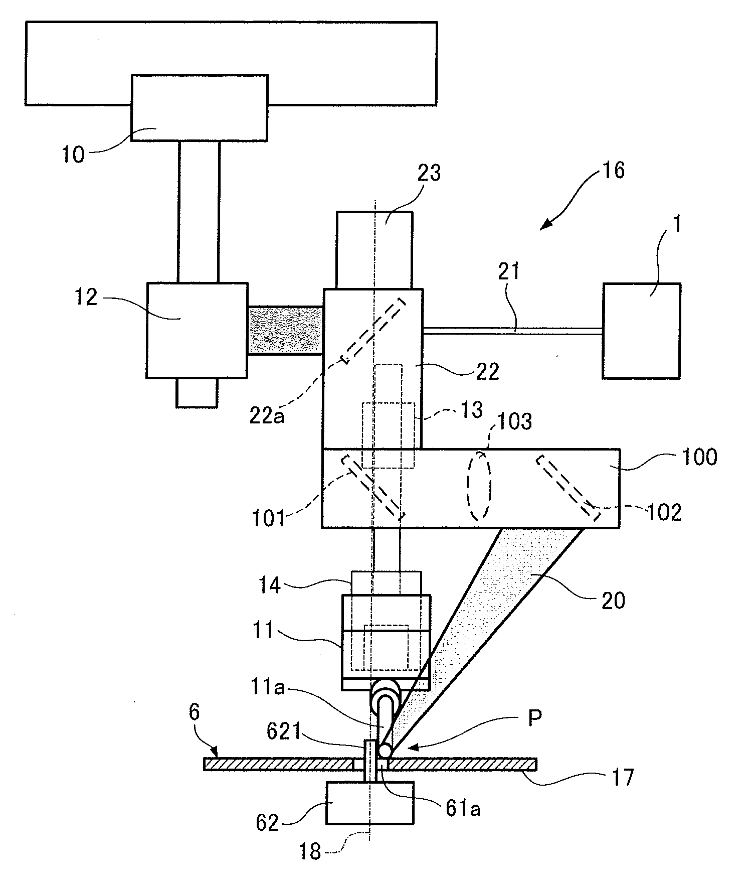
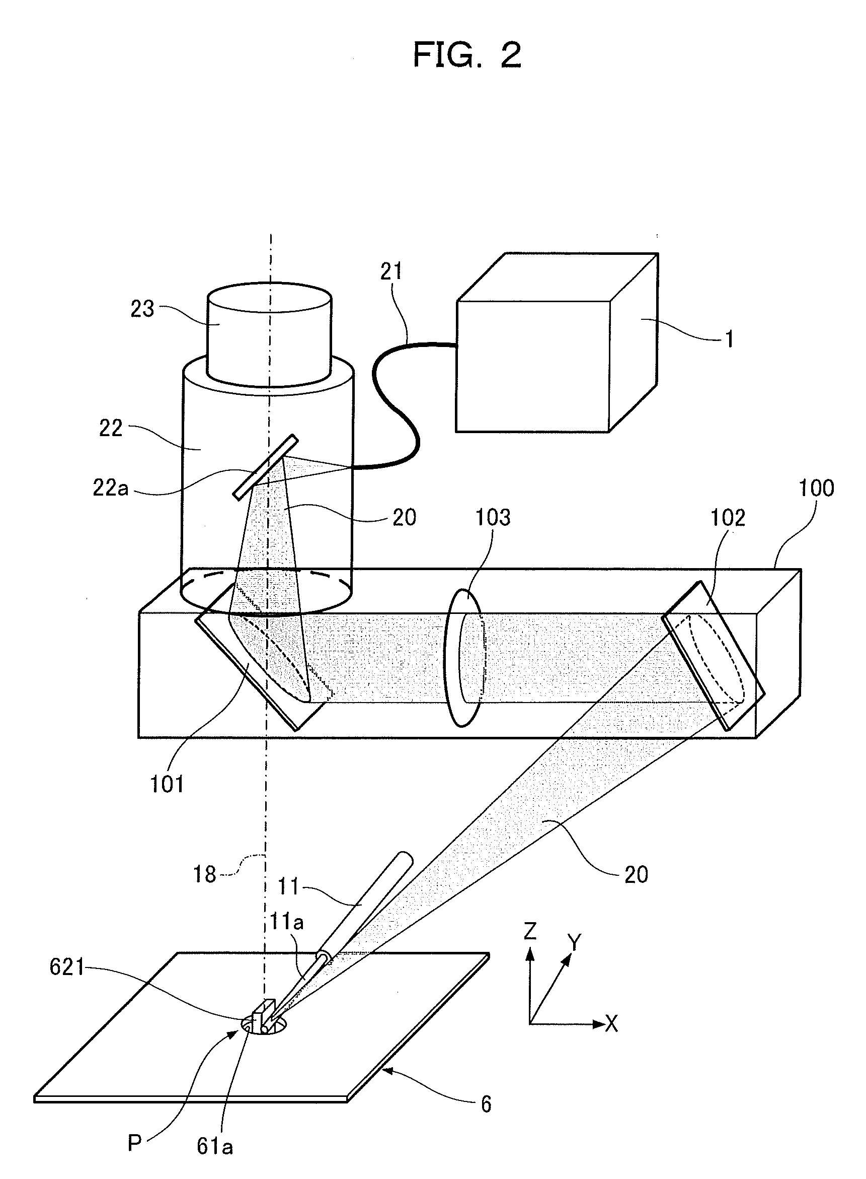
[0044]FIG. 1 shows a laser soldering apparatus according to the first embodiment.
[0045]Solder 11a is supplied from a solder supply unit 11 to a soldering point P on a substrate 6, in addition to which laser light 20 is irradiated at an irradiation angle of 11° to 76° with respect to the perpendicular direction onto the soldering point P.
[0046]At the soldering point P on the substrate 6, a flat insertion pin 621 serving as the lead of a component 62 is inserted into an insertion hole 61a formed on the substrate 6 from the side of a component mounting surface 17, and a through hole land 611 is formed about the insertion hole 61a as shown in FIG. 3A. Here, a material with low heat resistance, such as resin, is used for the component 62. The component 62 having low heat resistance is a component having a lower heat resistance limit than the melting point of the solder 11a.
[0047]A processing head 16 for irr...
second embodiment
[0067]In the first embodiment, the position of the condensing lens 103 in the reflective optics unit 100 is fixed to a previously determined position, but in this second embodiment, as shown in FIG. 6, a lens drive device 220 is provided to move the condensing lens 103 in the optical axis direction, from the position indicated by the solid lines to the position indicated by the virtual lines inside the reflective optics unit 100. Apart from this, the embodiment is the same as the first embodiment.
[0068]With this composition, by changing the position of the condensing lens 103 on a case-by-case basis in accordance with the shapes of an insertion hole 61a at a soldering point P, a through hole land 611 and an insertion pin 621, it is possible to obtain a spot shape 201 of an optimal mode. More specifically, it is possible to change the size of the spot shape 201 of the laser light 20 irradiated onto the soldering point P while being kept in a circle. The spot shape 201 is enlarged as ...
third embodiment
[0069]In the first embodiment, the position of the condensing lens 103 in the reflective optics unit 100 is fixed to a predetermined position, but in this third embodiment, a lens lacking axial symmetry optically, for instance, a cylindrical lens 104, is further provided between a first mirror 101 and a second mirror 102 of the reflective optics unit 100, as shown in FIG. 7. The cylindrical lens 104 can be inserted into and removed from the optical axis of the reflective optics unit 100 by an insertion drive device 230. Other compositions in the embodiment are the same as in the first embodiment.
[0070]With this composition, a line-shaped spot shape 202 can be obtained and it is possible to perform continuous soldering (liner Soldering) on the pin portion of a straight line-shaped component 62 arranged on a substrate 6. The length in the lengthways direction of the line-shaped spot shape 202 obtained at this point is in the range of 1 mm to 15 mm, for example, and the widthways direc...
PUM
| Property | Measurement | Unit |
|---|---|---|
| Angle | aaaaa | aaaaa |
| Angle | aaaaa | aaaaa |
| Temperature | aaaaa | aaaaa |
Abstract
Description
Claims
Application Information