Solid-state image sensor

a solid-state image and sensor technology, applied in the field of solid-state image sensors, can solve the problems of over-exceeding the upper limit of heat radiation, large power consumption, and high power consumption, and achieve the effects of suppressing power consumption, high speed, and high speed

Active Publication Date: 2010-08-19
TOHOKU UNIV +1
View PDF20 Cites 26 Cited by
  • Summary
  • Abstract
  • Description
  • Claims
  • Application Information

AI Technical Summary

Benefits of technology

[0055]The solid-state image sensors according to the first and second aspects of the present invention can achieve high-speed operations while suppressing the power consumption; for example, it is possible to ensure an adequately large number of continuously recordable frames for a high-speed operation that equals or exceeds one million frames per second. Thus, the imaging operation can be performed at higher speeds than in the case of the conventional solid-state image sensors, and useful information for the analysis of high-speed phenomena can be obtained. Since the deterioration of signals due to an intrusion of dark charges or excessive photocharges is alleviated, the SN ratio is improved, so that the images obtained by the high-speed imaging operation will have better qualities.

Problems solved by technology

(1) The aforementioned in-situ storage image sensor inherently consumes a large amount of power. This is because the gate electrodes and signal lines, both having high capacitive loads, must be simultaneously driven during the process of transferring signal charges to the CCD, and also because the voltage amplitude of the gate-driving signal is large. Attempting to increase the drive speed for higher imaging speeds would additionally increase the power consumption and possibly cause heat generation that exceeds the upper limit of heat radiation. Furthermore, the high capacitive load may cause waveform distortion of the drive signal (e.g. unsharpening of the waveform), in which case the attempt of increasing the imaging speed may totally prevent the charge transfer.
(2) In the aforementioned in-situ storage image sensor, the storage CCDs are located between the neighboring photodiodes on a semiconductor chip. Therefore, when a large amount of phortocharges are generated by an incidence of strong light onto a photodiode, some of the photocharges may flow into the storage CCD. As a result, various problems can occur, such as the deterioration of signal-to-noise (S / N) ratio of the images. In the worst case scenario, the image will be doubly produced.
(3) Even during the stand-by period for the next signal-reading cycle, the storage CCDs receive false signals due to dark charges. This may possibly lower the S / N ratio of the images.
Although this device can continuously record a few to several frames, it cannot perform the continuous imaging operation over such a large number of frames that the aforementioned high-speed imaging device is intended for.
Using more memory capacitors to increase the number of continuously recordable frames results in a higher capacitive load of the signal lines extending from the detection node storing the charges produced by the photodiode, which makes it difficult to raise the operation speed.
Furthermore, the area of the photodiode within each pixel inevitably decreases, which lowers the aperture ratio and accordingly deteriorates the sensitivity.Patent Document 1: Japanese Unexamined Patent Application Publication No. 2001-345441Patent Document 2: Japanese Unexamined Patent Application Publication (Translation of PCT Application) No. 2002-512461Non-Patent Document 1: Kondo et al., “Kousokudo Bideo Kamera HyperVision HPV-1 no Kaihatsu (Development of “HyperVision HPV-1” High-Speed Video Camera)”, Shimadzu Hyouron (Shimadzu Review), Shimadzu Hyouron Henshuu-bu, Sep. 30, 2005, Vol. 62, No. 1 / 2, pp.

Method used


Image

  • Solid-state image sensor
  • Solid-state image sensor
  • Solid-state image sensor

Examples


Embodiment Construction

[0106]A solid-state image sensor which is an embodiment of the present invention is hereinafter described with reference to the drawings.

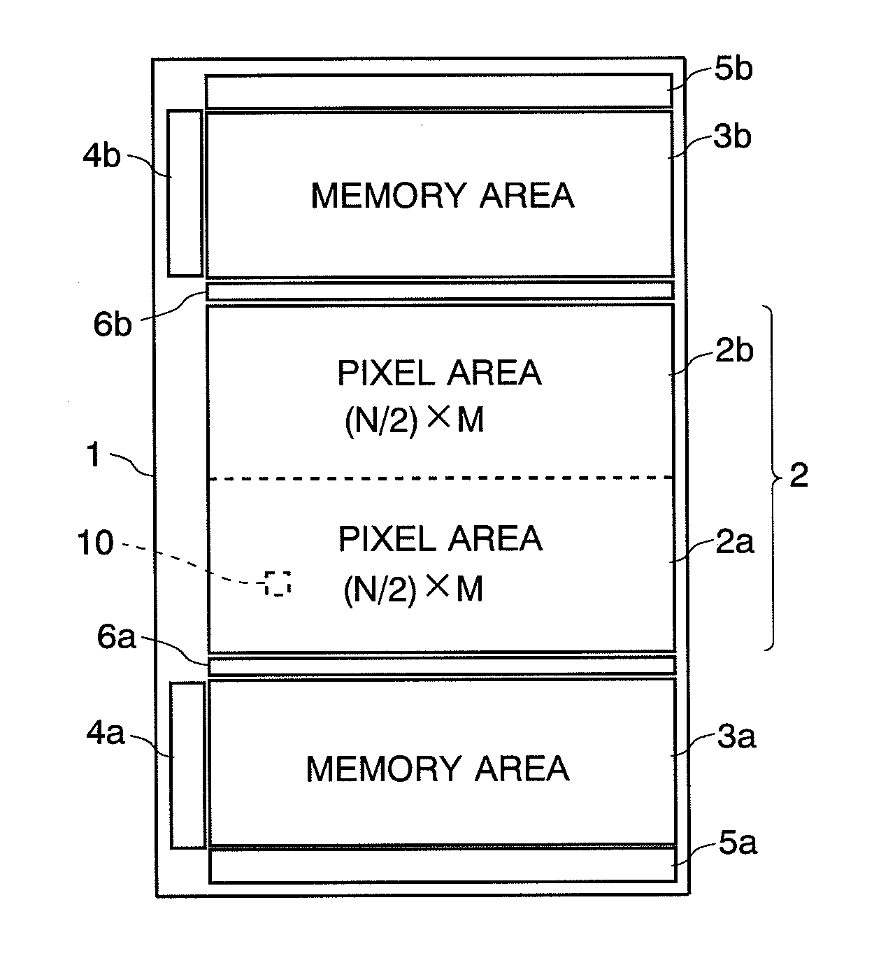
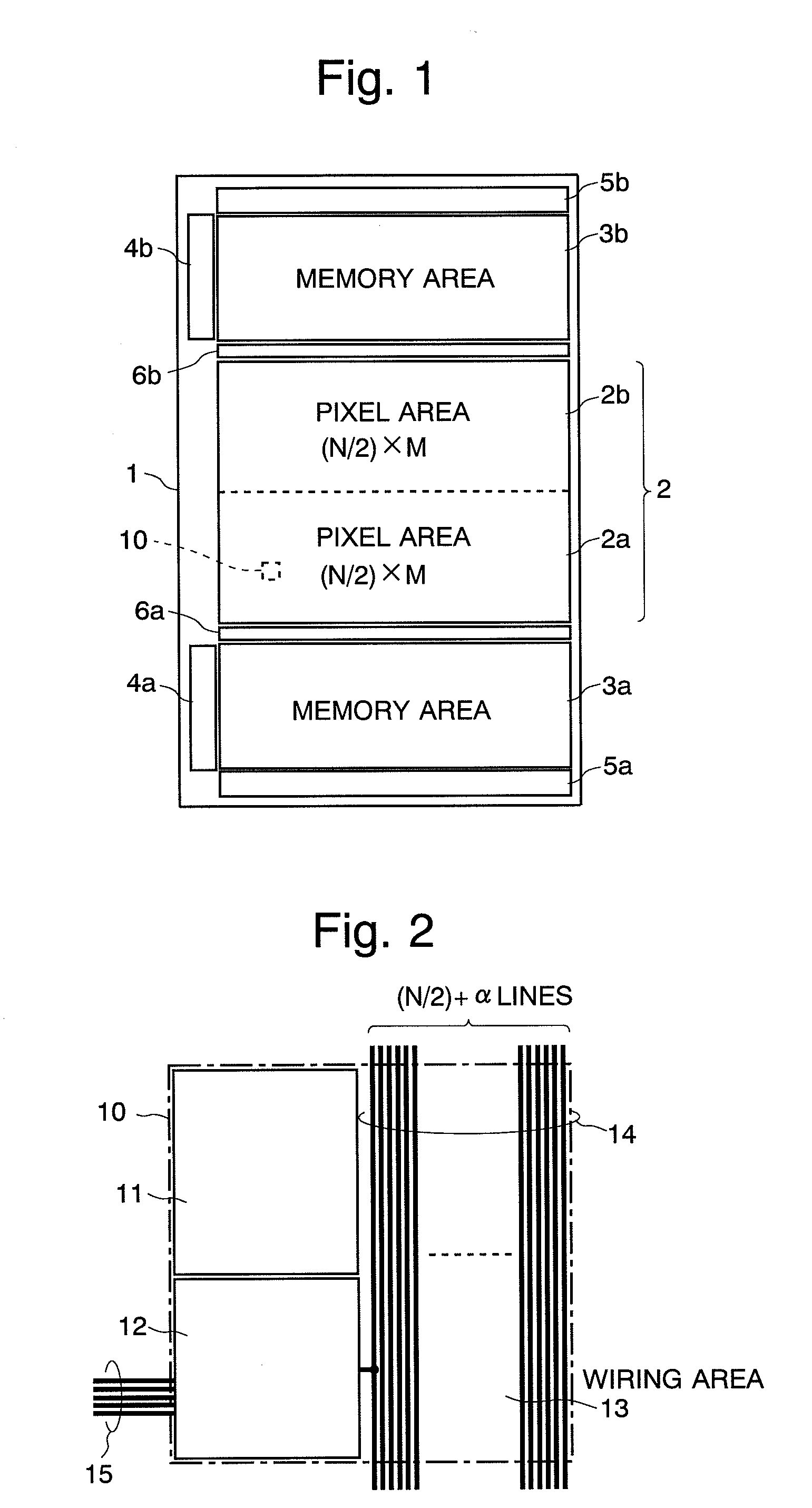
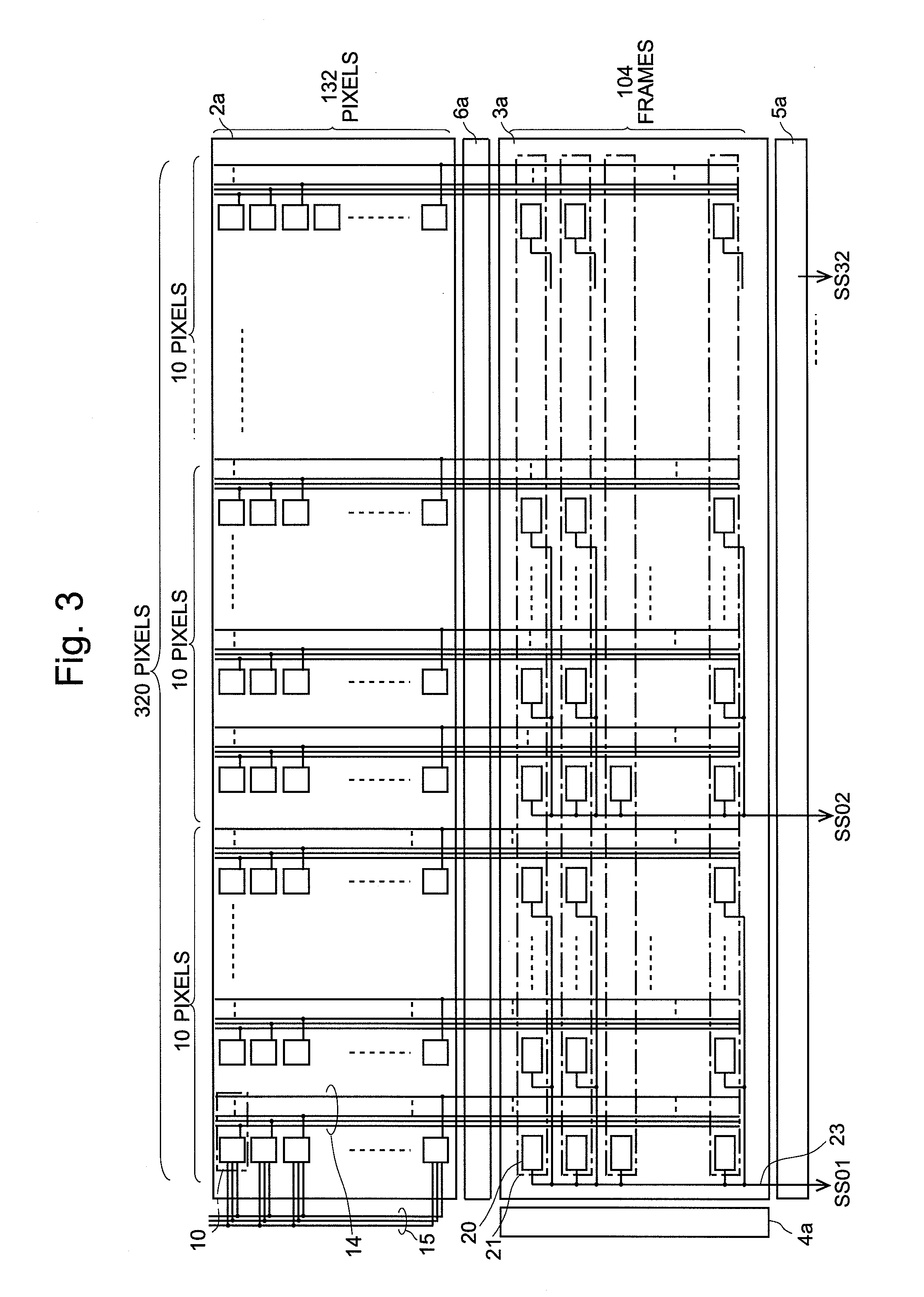
[0107]An overall configuration and structure of the solid-state image sensor according to the present embodiment is initially described. FIG. 1 is a plan view showing the schematic layout on a semiconductor chip of the solid-state image sensor of the present embodiment, and FIG. 3 is a block diagram of the main portion in the solid-state image sensor of the present embodiment.

[0108]As shown in FIG. 1, in the present solid-state image sensor, the pixel area 2 (2a and 2b) for receiving light and producing signals for each pixel and the memory areas 3a and 3b for holding the signals for a predetermined number of frames are not intermixed but completely separated from each other on the semiconductor substrate 1 so that each area forms a definite block. Within the rectangular pixel area 2, a total of N×M pixels 10 consisting of N rows and M columns are ...


PUM


Abstract

A pixel area with a two-dimensional array of pixels (10) each including a photodiode and a memory area (3a) on which memory sections for holding signals produced by the pixels for continuously recordable frames are separately provided on a semiconductor substrate. All the pixels simultaneously perform a photocharge storage operation, and the signals produced by the photocharge storage are extracted in parallel through mutually independent pixel output lines (14). In a plurality of memory sections connected to one pixel output line, a sample-and-hold transistor of a different memory section is turned on for each exposure cycle so as to sequentially hold signals in a capacitor of each memory section. After the continuous imaging is completed, all the pixel are sequentially read. Unlike CCD cameras, the present sensor does not simultaneously drive all the gate loads. Therefore, the sensor consumes less power yet can be driven at high speeds. The separation between the memory area and pixel area prevents signals from deterioration due to an intrusion of excessive photocharges. As a result, the sensor can perform imaging operations at higher speeds than ever before and yet capture images with higher qualities.

Description

TECHNICAL FIELD[0001]The present invention relates to a solid-state image sensor and, more specifically, to a solid-state image sensor capable of high-speed operations suitable for taking images of high-speed phenomena such as destructions, explosions and combustions.BACKGROUND ART[0002]High-speed imaging devices (high-speed video cameras) for taking consecutive images of high-speed phenomena such as explosions, destructions, combustions, collisions and discharges for only a short period of time have been conventionally developed (for example, refer to Non-Patent Document 1 and other documents). Such high-speed imaging devices need to perform an ultrahigh-speed imaging operation that exceeds a level of approximately one million images per second. Accordingly, they use solid-state image sensors capable of high-speed operations, which have special structures different from those of the imaging devices used in normal video cameras, digital cameras and similar devices.[0003]One example ...

Claims


Application Information

Patent Timeline
Patent Type & Authority Applications(United States)
IPC IPC(8): H04N5/335H04N5/355H04N5/3745
CPCH04N5/35527H04N5/378H04N5/37452H04N25/575H04N25/771H04N25/75
Inventor SUGAWA, SHIGETOSHIKONDO, YASUSHITOMINAGA, HIDEKI
Owner TOHOKU UNIV
Why Eureka
Try Eureka