Use of design information and defect image information in defect classification

Active Publication Date: 2010-08-19
KLA TENCOR TECH CORP
View PDF6 Cites 47 Cited by
  • Summary
  • Abstract
  • Description
  • Claims
  • Application Information

AI Technical Summary

Benefits of technology

[0068]Defect classification may be implemented by comparing the defect image to the synthetic reference image to build a subset of feature vectors for later analysis. However, if a synthetic reference image is used it is not necessary to separately collect a reference image with the defect inspection tool. This allows an existing defect classification scheme to be implemented in a way that utilizes design information. This allows an existing defect classification full detection and classification capabilities while maintaining high throughput since a synthetic reference image can be generated much more quickly than a normal reference image.
[0069]The synthetic reference i

Problems solved by technology

However, the review tool is often different from the inspection tool used to locate the defects.
One drawback to this method is that the classification is only based on comparison to prior defects.
The system therefore has no knowledge of the actual design of the devices to be formed on the waf

Method used


Image

  • Use of design information and defect image information in defect classification
  • Use of design information and defect image information in defect classification
  • Use of design information and defect image information in defect classification

Examples


Embodiment Construction

[0012]Although the following detailed description contains many specific details for the purposes of illustration, anyone of ordinary skill in the art will appreciate that many variations and alterations to the following details are Within the scope of the invention. Accordingly, the exemplary embodiments of the invention described below are set forth without any loss of generality to, and without imposing limitations upon, the claimed invention.

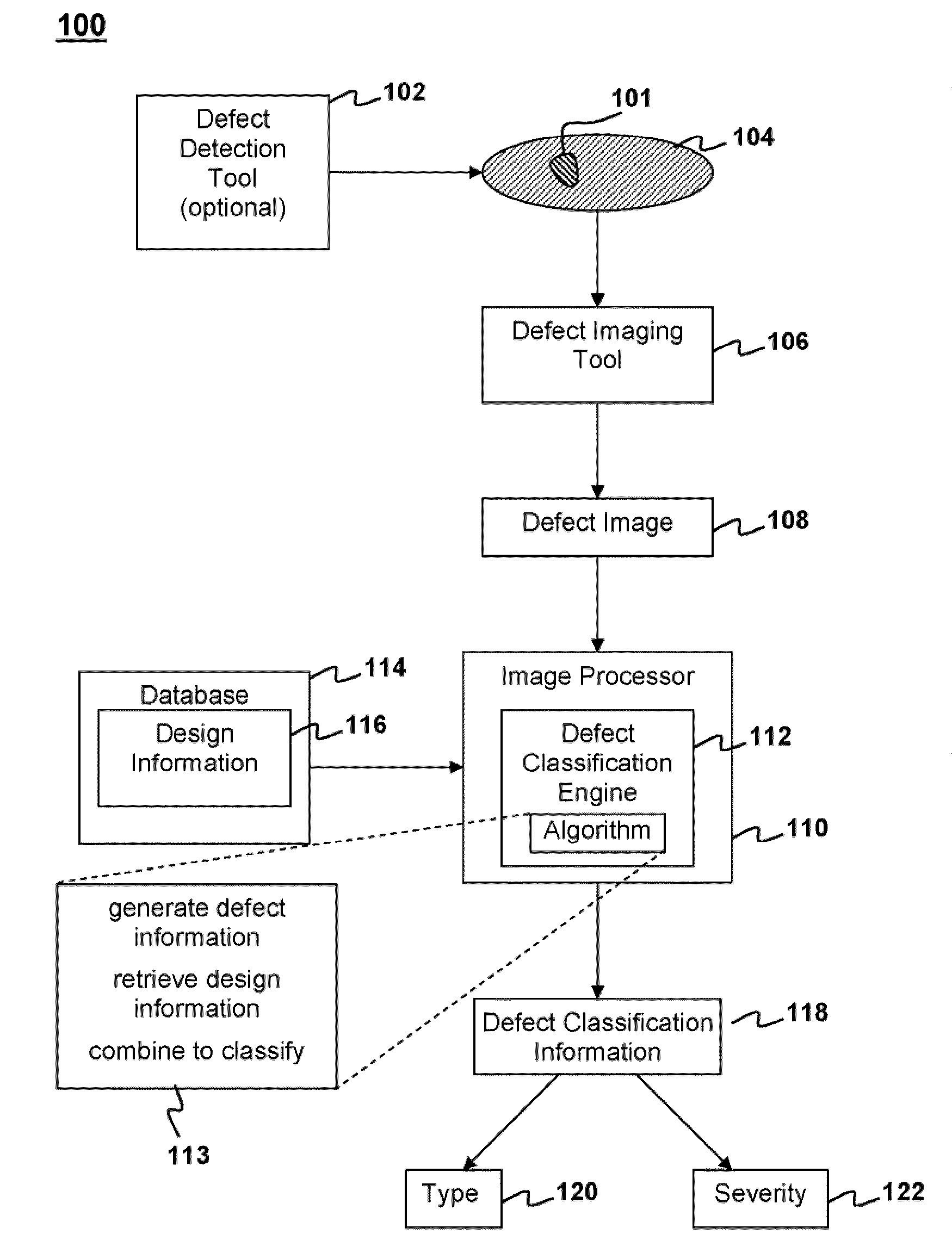
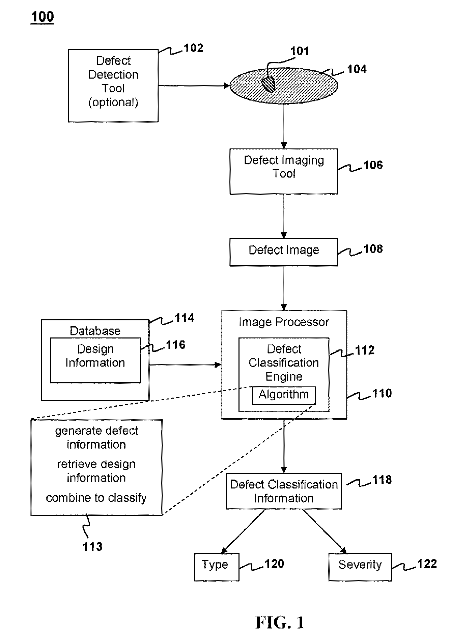
[0013]FIG. 1 is a flow diagram illustrating a process 100 for defect classification based only on a single defect image and the design information or a semiconductor device according to an embodiment of the present invention. As shown in FIG. 1, a defect 101 on a wafer 104 is optionally detected using a defect detection tool 102.

[0014]A defect imaging tool 106 may then generate a defect image 108 of the defect 101. The defect imaging tool 106 may be SEM, CD-SEM, AFM, STM, optical microscope and the like. An example of a commercially availabl...


PUM


Abstract

Defects observed by imaging tools may be classified by automatic comparison of features observed in a defect image with design information relating to corresponding portions of the image. Defect information may be generated from a defect image from a defect imaging tool. Design information relating to one or more structures to be formed on the substrate in a vicinity of the defect may be retrieved. The defect may be classified based on a combination of the defect information from the defect image and design information relating to one or more structures to be formed on the substrate in the vicinity of the defect.

Description

FIELD OF THE INVENTION[0001]This invention generally relates detecting and classifying defects for a semiconductor device and more particularly to methods for doing image-based defect classification based on a defect image and design information.BACKGROUND OF THE INVENTION[0002]As is well known, considerable effort is spent in academia and industry towards developing techniques enabling the detection of defects in wafers before their cleavage into distinct dies, capsulation and subsequent distribution to the marketplace in the form of chips. In recent years, defect detection has been improved by techniques for classifying defects into distinct defect types. These techniques not only allow identification of defective wafers so as to increase the yield, but also to provide some information on the cause of the defects. The production stage can then be reconfigured or modified in order to produce a better wafer series.[0003]A conventional method for defect classification called Automati...

Claims


Application Information

Patent Timeline
IPC IPC(8): G06K9/00G06K9/62
CPCG06K2209/19G06T2207/30148G06T2207/10061G06T7/0006G06V2201/06
Inventor ABBOTT, GORDONFOUQUET, CHRISTOPHETADMOR, ORITADA, TAKUJI
Owner KLA TENCOR TECH CORP
Why Eureka
Try Eureka